
PCB Surface Finish: Hot Air Solder Leveling (HASL) Process
Abstract
Hot Air Solder Leveling (HASL), also known as Hot Air Leveling (HAL), is a widely used surface finish technology in printed circuit board (PCB) manufacturing. It involves coating exposed copper surfaces with a layer of molten solder (typically tin-lead or lead-free alloys) and then using hot air to level the solder, ensuring a flat and uniform surface. This process enhances solderability, protects copper from oxidation, and improves the reliability of PCB assemblies. This article explores the HASL process, its advantages, limitations, process steps, and comparisons with alternative surface finishes.
1. Introduction
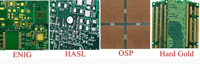
Surface finishes in PCB manufacturing play a critical role in ensuring reliable electrical connections, protecting copper traces from oxidation, and facilitating component soldering. Among various surface finish techniques, Hot Air Solder Leveling (HASL) remains one of the most cost-effective and widely adopted methods, particularly in consumer electronics, industrial controls, and automotive applications.
HASL involves applying molten solder to the PCB’s copper pads and then using hot air knives to remove excess solder, leaving a thin, even coating. This article provides a detailed examination of the HASL process, including its variations (lead-based and lead-free), process steps, advantages, and challenges.
2. HASL Process Overview
The HASL process consists of several key steps:
2.1. PCB Cleaning and Preparation
Before applying solder, the PCB must be thoroughly cleaned to remove contaminants such as oxides, dust, and residues from previous manufacturing steps. Common cleaning methods include:
- Chemical cleaning (acid or alkaline solutions)
- Mechanical abrasion (brushing or micro-etching)
- Water rinsing and drying
2.2. Flux Application
A flux is applied to the PCB to promote solder adhesion and prevent oxidation during the soldering process. Common flux types include:
- Rosin-based fluxes (for lead-based solders)
- No-clean fluxes (for lead-free solders)
- Water-soluble fluxes (easier to clean but require post-treatment)
2.3. Solder Dipping
The PCB is immersed in a molten solder bath (typically at 250–270°C for lead-based solder or 260–280°C for lead-free solder). The solder adheres to exposed copper surfaces, including pads, through-holes, and vias.
2.4. Hot Air Leveling
After solder dipping, the PCB passes through hot air knives that blow high-pressure hot air (typically 300–400°C) to remove excess solder, ensuring a smooth and uniform coating. This step is critical for preventing solder bridging and uneven surfaces.
2.5. Cooling and Inspection
The PCB is cooled, and the solder solidifies. Post-HASL inspection includes:
- Visual inspection (for solder uniformity, bridging, or defects)
- Thickness measurement (typically 1–40 μm)
- Solderability testing (wetting balance or dip-and-look tests)
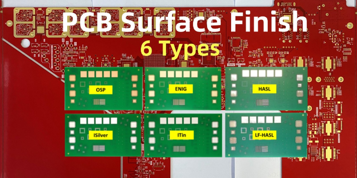
3. Types of HASL: Lead-Based vs. Lead-Free
3.1. Lead-Based HASL (Sn-Pb)
- Composition: 63% tin (Sn) and 37% lead (Pb) (eutectic alloy)
- Advantages:
- Excellent solderability and wetting properties
- Lower melting point (183°C) reduces thermal stress on PCBs
- Cost-effective and widely available
- Disadvantages:
- Environmental and health concerns (RoHS restrictions)
- Not suitable for high-reliability or medical applications
3.2. Lead-Free HASL (Sn-Cu, Sn-Ag-Cu, etc.)
- Common Alloys:
- SAC305 (Sn96.5-Ag3.0-Cu0.5)
- Sn-Cu (Sn99.3-Cu0.7)
- Advantages:
- RoHS-compliant and environmentally friendly
- Better thermal fatigue resistance than Sn-Pb
- Disadvantages:
- Higher melting point (217–227°C) increases thermal stress
- Potential for tin whiskers (requires additional mitigation)
- Less uniform coating due to higher surface tension
4. Advantages of HASL
- Cost-Effectiveness: Lower material and processing costs compared to ENIG or immersion silver.
- Excellent Solderability: Provides a highly solderable surface for component assembly.
- Long Shelf Life: Protects copper from oxidation for extended periods (6–12 months).
- Repairability: Easily reworkable compared to some alternative finishes.
- Wide Industry Adoption: Proven reliability in consumer and industrial applications.
5. Limitations and Challenges
- Thermal Stress: High temperatures during HASL can damage sensitive components or thin PCBs.
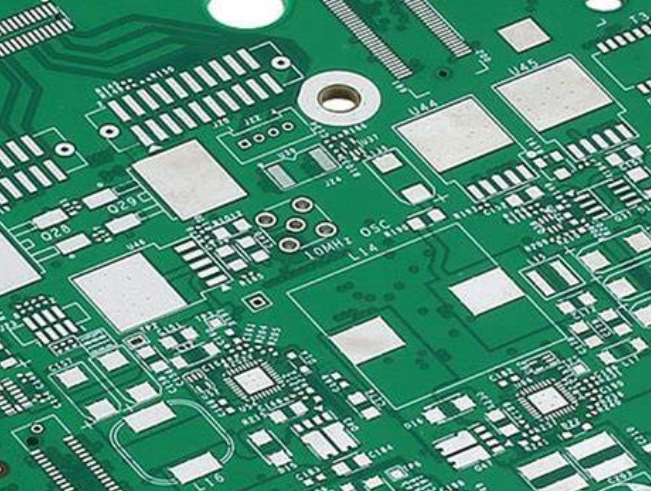
- Uneven Surface: Thicker solder deposits may cause planarity issues for fine-pitch components.
- Environmental Concerns: Lead-based HASL is restricted under RoHS (except for exemptions).
- Solder Bridging Risk: Requires precise control of air knife pressure and temperature.
- Not Suitable for HDI PCBs: Limited compatibility with ultra-fine pitch and microvia designs.
6. Comparison with Alternative Surface Finishes
| Finish Type | Thickness (μm) | Solderability | Planarity | Cost | RoHS Compliance |
|---|---|---|---|---|---|
| HASL (Sn-Pb) | 1–40 | Excellent | Moderate | Low | No |
| HASL (Lead-Free) | 1–40 | Good | Moderate | Low | Yes |
| ENIG (Ni/Au) | 3–6 Ni / 0.05–0.1 Au | Excellent | High | High | Yes |
| Immersion Silver | 0.1–0.5 | Good | High | Medium | Yes |
| OSP | 0.2–0.5 | Fair | High | Low | Yes |
| Immersion Tin | 0.8–1.2 | Good | High | Medium | Yes |
7. Applications of HASL
HASL is commonly used in:
- Consumer electronics (TVs, home appliances)
- Industrial control systems
- Automotive electronics (non-safety-critical PCBs)
- Power supply boards
- LED lighting circuits
However, for high-density interconnect (HDI) PCBs or advanced packaging, alternatives like ENIG or immersion silver are preferred.
8. Future Trends and Improvements
- Advanced Lead-Free Alloys: Development of low-temperature lead-free solders to reduce thermal stress.
- Selective HASL: Applying solder only to specific areas to improve planarity.
- Automated Quality Control: AI-based inspection systems for defect detection.
- Hybrid Finishes: Combining HASL with OSP or ENIG for enhanced performance.
9. Conclusion
HASL remains a dominant PCB surface finish due to its cost-effectiveness, excellent solderability, and reliability. While lead-free HASL has gained traction due to environmental regulations, challenges such as thermal stress and uneven coating persist. Engineers must carefully select HASL or alternative finishes based on application requirements, component density, and compliance standards.
As PCB technology evolves, advancements in HASL processes and materials will continue to enhance its viability in modern electronics manufacturing.