
Peelable Solder Mask: Temporary Protection for Gold Fingers and Test Points
Wave soldering and selective soldering processes can contaminate critical PCB areas like gold fingers, test points, and connectors with unwanted solder. According to industry data, 15-25% of assembly rework stems from solder contamination on protected contact areas. Peelable solder mask provides temporary, high-temperature protection that removes cleanly after soldering operations.
This technical guide covers peelable mask applications, material types, application methods, and removal techniques to help hardware engineers and PCBA managers select the right temporary masking solution for their projects.
What Is Peelable Solder Mask?
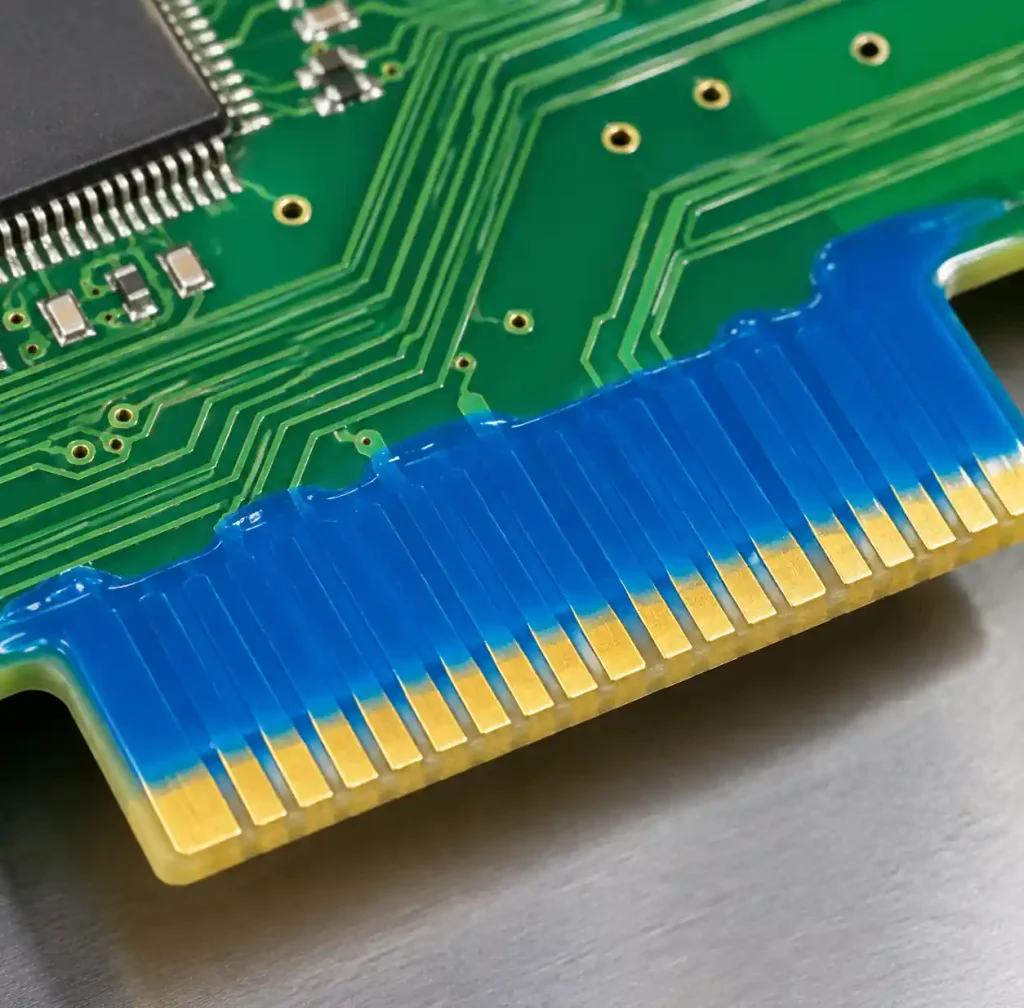
Peelable solder mask is a temporary protective coating applied to specific PCB areas before wave soldering, selective soldering, or conformal coating operations. Unlike permanent solder mask (the green coating on finished boards), peelable mask is designed to be removed manually after the soldering process completes.
The material forms a high-temperature resistant barrier that protects gold fingers, edge connectors, plated-through holes, test points, and other contact surfaces from molten solder, flux residue, and cleaning fluids. Typical formulations withstand temperatures up to 268°C (515°F) for 10-60 seconds during wave soldering exposure.
You can apply peelable mask through screen printing, dispensing, or manual brush application depending on production volume and precision requirements. The coating cures to a rubbery consistency that peels off as a single film, leaving no residue on copper, gold, or pre-tinned surfaces.
Peelable Mask Applications in PCB Assembly
Gold Finger Protection
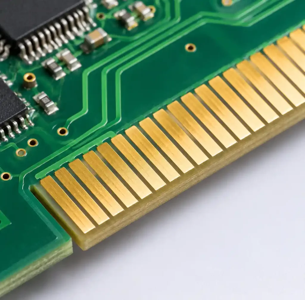
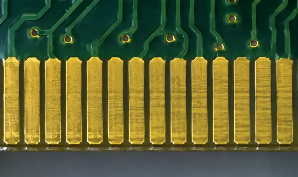
Gold fingers (edge connector contacts) require protection during board assembly and soldering operations. Wave soldering or selective soldering can deposit solder on gold-plated contacts, degrading signal integrity and preventing proper insertion into mating connectors.
You should apply peelable mask to gold finger areas before the soldering process. The mask prevents solder wicking onto the plated contacts while allowing other board areas to receive solder. After soldering, remove the mask to expose clean, solder-free gold contacts ready for connector insertion.
Test Point Masking
Test points and probe pads need protection during selective soldering operations. Solder contamination on test points interferes with in-circuit testing (ICT) and flying probe testing, requiring manual cleaning or rework that increases assembly costs.
Peelable mask keeps test points clean and accessible for automated testing equipment. This is especially critical for dense PCBs where test points sit close to soldered components. The mask ensures reliable electrical contact during testing without cleaning operations.
Selective Wave Soldering
During selective wave soldering, only specific board areas pass through the solder wave while other regions must remain solder-free. Peelable mask defines these protected zones more precisely than mechanical fixtures or nitrogen knives.
You can mask SMT component areas on mixed-technology boards where through-hole components require wave soldering but surface-mount devices have already been reflowed. The mask prevents solder splash and bridging on SMT pads, eliminating the need for secondary cleaning.
Connector and Socket Protection
Multi-pin connectors and IC sockets need protection during board-level soldering when mounted before the soldering operation. Solder contamination inside connector housings or socket contacts causes intermittent connections and field failures.
Apply peelable mask to connector openings and socket cavities before wave or selective soldering. The mask fills voids and creates a physical barrier against solder intrusion. After soldering, remove the mask to restore full connector functionality.
Material Types and Properties
| Material Type | Base Chemistry | Temperature Resistance | Removal Method | Shelf Life | Best Application |
|---|---|---|---|---|---|
| Latex-Based | Natural rubber latex | Up to 260°C (500°F) | Manual peel | 6-12 months | Wave soldering, high-volume |
| Synthetic Latex | Acrylic/styrene polymer | Up to 268°C (515°F) | Manual peel | 12-18 months | Selective soldering, no ammonia |
| Silicone-Based | Silicone elastomer | Up to 300°C (572°F) | Manual peel | 18-24 months | High-temperature applications |
| Water-Soluble | Polyvinyl alcohol | Up to 250°C (482°F) | Water rinse | 6-9 months | Automated removal, high-volume |
| Alcohol-Soluble | Modified acrylic | Up to 260°C (500°F) | IPA rinse | 12-15 months | Fine-pitch protection |
Latex-Based Masks
Natural latex formulations provide the lowest cost per application and work well for standard wave soldering operations at 250-260°C. The material cures through solvent evaporation in 10-30 minutes at room temperature, forming a flexible film 0.05-0.15mm thick.
Latex masks contain ammonia as a stabilizer, which can corrode exposed copper over extended periods (24+ hours). Apply latex mask shortly before soldering and remove it within 48 hours to prevent copper oxidation. The material works best on flat surfaces and may not penetrate small through-holes effectively.
Synthetic Latex Masks
Synthetic latex eliminates ammonia content while maintaining high-temperature resistance and peel characteristics. These formulations use acrylic or styrene-based polymers that cure to a non-corrosive film suitable for extended masking periods (up to 7 days on board).
Synthetic masks cost 15-30% more than natural latex but offer better chemical resistance and longer shelf life. You can use synthetic masks on pre-tinned surfaces, ENIG finishes, and immersion silver without risking surface contamination.
Silicone-Based Masks
Silicone elastomer masks handle the highest temperatures (up to 300°C) and provide the best chemical resistance for harsh flux formulations or aggressive cleaning solvents. The material remains flexible after thermal cycling and works well for masking irregular surfaces or 3D features.
Silicone masks require 30-60 minutes curing time and cost 2-3× more than latex formulations. They are preferred for selective soldering applications where extended dwell time at high temperatures occurs, such as thick PCBs with heavy copper or multilayer boards requiring multiple solder passes.
Application Methods
Screen Printing Application
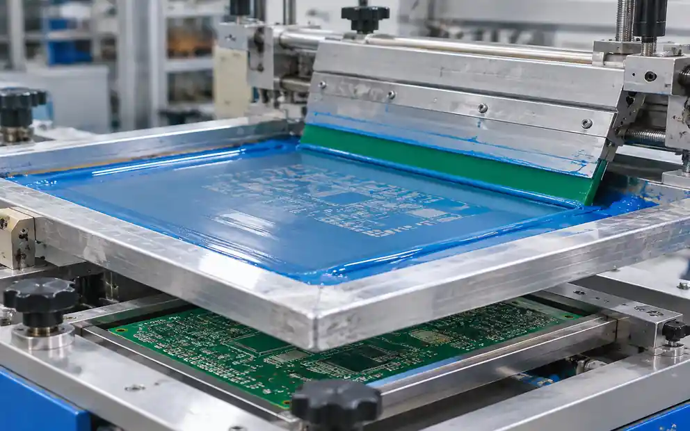
Screen printing provides the most consistent and repeatable peelable mask application for medium to high-volume production (500+ boards per month). The process uses a mesh screen with open areas corresponding to the regions requiring mask coverage.
Typical screen specifications include 230-305 mesh count with 15-25 micron emulsion thickness. Squeegee pressure ranges from 40-60 degrees hardness with 45-60 degree attack angle. Print speeds of 50-100mm/second produce optimal film thickness of 75-150 microns per pass.
Screen printing works best for simple geometric shapes like gold finger strips, connector areas, and test point groups. The method achieves ±0.1mm placement accuracy and provides excellent thickness uniformity across the board.
Dispensing Application
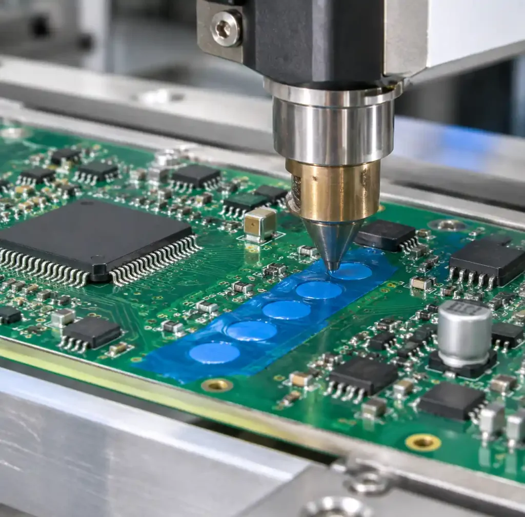
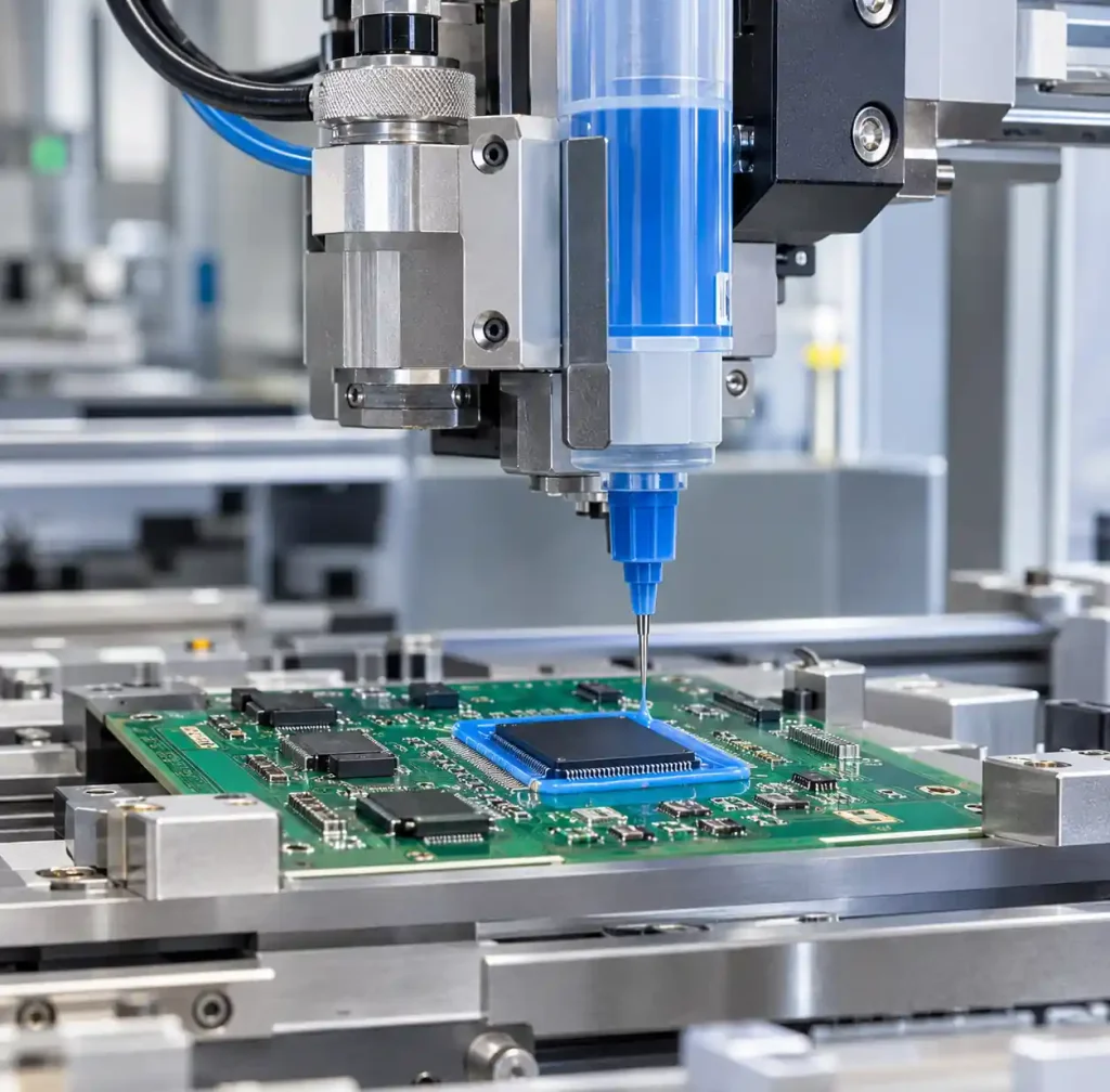
Automated dispensing systems apply peelable mask through pneumatic or auger-driven dispensers with 0.5-2.0mm diameter tips. This method suits low-volume production (50-500 boards per month) and complex masking patterns that change frequently.
You can program dispense paths using CAD data, eliminating custom screen costs for each design. Typical dispense speeds range from 25-75mm/second with 0.05-0.15mm height resolution. The system controls material flow rate, dispense pressure, and valve timing to produce consistent bead width and height.
Dispensing provides superior coverage for small through-holes and narrow gaps between components compared to screen printing. The method requires 15-45 minute setup time per new board design versus 2-4 hour screen fabrication lead time.
Manual Brush Application
Manual brush application serves prototype builds, rework operations, and very low-volume production (1-50 boards). Use synthetic bristle brushes (8-15mm width) with medium stiffness to apply the mask evenly across target areas.
Apply mask in 2-3 thin coats rather than one thick layer to prevent air bubbles and ensure complete coverage. Each coat should cure 80% (touch-dry) before applying the next layer. Final film thickness should reach 100-200 microns for reliable high-temperature protection.
Manual application provides maximum flexibility for irregular shapes and selective coverage but shows higher thickness variation (±30%) compared to automated methods. This approach works well for masking individual gold fingers or small connector groups during board rework.
Removal Process and Best Practices
Manual Peel Removal
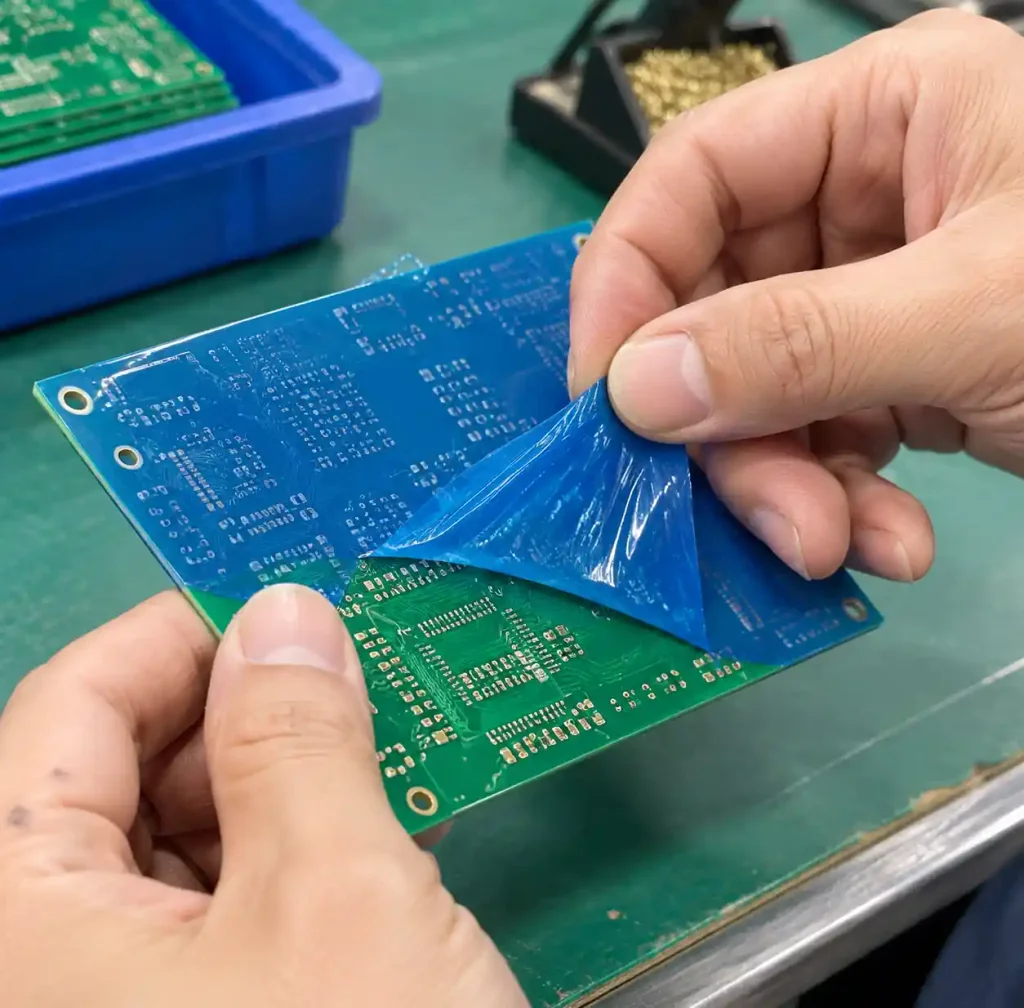
Manual peeling is the standard removal method for latex and synthetic peelable masks. The mask should lift as a continuous film without tearing or leaving residue. Start the peel from a corner or edge, pulling at a 45-90 degree angle relative to the board surface.
Optimal peel occurs within 24-72 hours after soldering while the mask retains flexibility. Aged mask (7+ days) becomes brittle and may fragment during removal, leaving small pieces adhered to the board. If the mask fragments, apply fresh mask over the residue, allow 15 minutes contact time, then peel both layers together.
Temperature affects peel characteristics significantly. Remove mask at 20-25°C (room temperature) for best results. Cold masks (below 10°C) become stiff and tear easily, while warm masks (above 35°C) may stretch and leave thin residue films.
Solvent Cleaning Removal
Water-soluble and alcohol-soluble masks require liquid cleaning for complete removal. Water-soluble masks dissolve in 40-60°C deionized water within 3-5 minutes of immersion, suitable for inline spray washing systems.
Alcohol-soluble masks respond to isopropyl alcohol (IPA) concentrations of 70-99%. Spray or immerse boards for 2-4 minutes, then rinse with clean IPA or DI water. This method works well when boards require cleaning for flux residue removal in the same process step.
Automated cleaning systems provide more consistent removal than manual peeling and eliminate labor costs for high-volume production. The cleaning process should include verification steps to confirm complete mask removal from holes and underside areas.
Residue Management
Peelable mask should remove cleanly without residue under normal conditions. Residue formation indicates improper application thickness, contaminated surfaces before masking, or expired material past shelf life.
If residue occurs, remove it using IPA wipes, industrial cleaners (flux removers), or adhesive removers compatible with the PCB finish. Avoid abrasive cleaning methods that could damage gold plating or solder mask surfaces. Test cleaning agents on a sample board first to verify compatibility.
Cost Comparison: Peelable Mask vs Alternatives
| Protection Method | Material Cost per Board | Application Time | Removal Time | Rework Difficulty | Temperature Limit |
|---|---|---|---|---|---|
| Peelable Mask | $0.15-0.80 | 1-3 minutes | 0.5-2 minutes | Low | 260-300°C |
| Kapton Tape | $0.50-1.50 | 3-5 minutes | 1-3 minutes | Moderate | 260°C |
| Aluminum Tape | $0.30-0.90 | 2-4 minutes | 1-3 minutes | Moderate | 300°C+ |
| Mechanical Fixtures | $50-500 (amortized) | 0.5-1 minute | 0.5-1 minute | High | Unlimited |
| Selective Tooling | $200-2000 (amortized) | 0 (automatic) | 0 (none needed) | Very High | Unlimited |
Peelable Mask Cost Analysis
Peelable mask material costs range from $40-120 per liter depending on formulation type. Screen-printed application at 75-100 micron wet thickness yields 8-12 square meters of coverage per liter, resulting in $0.15-0.45 per typical board (100×150mm with 30cm² masked area).
Labor costs add $0.10-0.35 per board for screen printing application and removal (2-4 minutes total cycle time at $15-25/hour labor rate). Total cost per board ranges from $0.25-0.80 for medium volume production.
Volume economics favor peelable mask over tape solutions above 200-300 boards per design due to lower per-unit material cost and faster application/removal cycles. Below 50 boards per design, tape may cost less when considering screen fabrication expenses ($100-200 per screen).
Alternative Methods
Kapton polyimide tape provides temperature resistance up to 260°C and removes without residue but costs 2-3× more than peelable mask per application. Tape application requires precise cutting and placement, consuming more labor time especially for complex patterns.
Mechanical fixtures offer reusable protection for very high-volume production (10,000+ boards) but require significant upfront investment ($50-500 per fixture) and limit design flexibility. Fixtures suit standardized designs with fixed masking areas that remain constant across production runs.
Selective soldering tooling eliminates masking requirements entirely by controlling solder wave contact with programmed nozzle movement. This approach requires substantial capital investment ($50,000-200,000+ for selective solder system) and works best for high-volume production where tooling costs amortize over large quantities.
Design Considerations for Peelable Mask
Mask Area Sizing
Design mask coverage areas 1.0-2.0mm larger than the critical features requiring protection. This clearance compensates for screen printing registration tolerance (±0.15mm) and ensures complete coverage during application.
For gold fingers, extend the mask 2-3mm beyond the contact area onto the non-functional board edge. This provides a gripping edge for peel removal and prevents mask from delaminating during handling. Leave 0.5-1.0mm unmasked strip along the board edge to facilitate starting the peel.
Through-Hole Masking
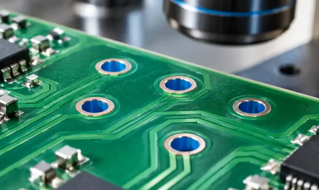
Mask must fully penetrate plated-through holes to prevent solder wicking from the backside during wave soldering. Screen printing may not fill holes smaller than 0.8mm diameter reliably, requiring dispensing or increased print thickness.
For 0.5-0.8mm holes requiring complete masking, apply mask from both board sides or use vacuum-assisted screen printing to pull material through the holes. Verify fill quality using transmitted light inspection before the soldering operation.
Board Finish Compatibility
Peelable mask adheres to all standard PCB finishes including HASL, ENIG, immersion silver, immersion tin, and OSP. Surface cleanliness critically affects adhesion and clean removal. Organic contamination (oils, fingerprints) prevents proper mask bonding and causes adhesion failures during soldering.
Clean boards with IPA or electronics cleaner immediately before mask application. Allow surfaces to dry completely (15-30 minutes) before applying mask. Verify cleanliness using water break test or contact angle measurement if adhesion problems occur repeatedly.
Temperature Profile Considerations
Match the peelable mask formulation to your soldering temperature profile. Standard latex masks handle 250-260°C peak temperatures for 3-10 seconds dwell time typical of wave soldering. Selective soldering with 10-30 second localized heating may require synthetic latex or silicone formulations.
Review the mask manufacturer’s technical datasheet for maximum temperature exposure time curves. Exceeding rated temperature or dwell time can cause mask charring, adhesive residue formation, or complete mask breakdown requiring extensive cleaning.
Quality Control and Verification
Application Inspection
Inspect mask coverage immediately after application and curing using visual inspection under 3-5× magnification. Look for complete coverage of protected areas, uniform thickness without thin spots, and proper adhesion to the board surface without bubbles or edge lifting.
Measure film thickness using wet film thickness gauges (for uncured mask) or dry film thickness gauges (after curing). Target thickness ranges from 100-150 microns for screen-printed applications. Thickness below 75 microns risks breakthrough during high-temperature exposure.
Critical applications (aerospace, medical, automotive) require documented thickness measurements at specified locations (corners, center, near through-holes) to verify process control. Record measurements in traveler documents or electronic manufacturing execution system (MES) for traceability.
Post-Removal Verification
After mask removal, inspect protected areas for complete cleanliness and absence of solder contamination. Use low-power microscopy (10-20×) to verify gold fingers, test points, and connector contacts remain solder-free and clean.
Check for mask residue using IPA wipe test or tape test. Press clean IPA-moistened wipe or transparent tape onto the previously masked area, then examine for material pickup indicating incomplete removal. Any residue requires additional cleaning before functional testing or shipment.
Perform electrical testing on gold fingers and test points after mask removal to verify proper contact resistance. Open or high-resistance measurements indicate solder contamination or residue requiring rework.
Frequently Asked Questions
How long can peelable mask remain on a PCB before removal becomes difficult?
Remove peelable mask within 24-72 hours after application for optimal peel characteristics. Latex and synthetic formulations remain flexible for 5-7 days but become increasingly brittle after 7+ days. Aged mask may fragment during removal or leave residue requiring solvent cleaning. If extended masking duration is necessary, choose silicone-based formulations that maintain flexibility for 10-14 days or water-soluble masks that remove easily regardless of age.
Can peelable mask protect against conformal coating overspray?
Yes, peelable mask effectively protects connectors, test points, and contact areas from conformal coating overspray during spray or dip coating operations. Apply mask before coating, cure completely, then proceed with conformal coating application. Remove mask after coating cures (per coating manufacturer’s specifications, typically 24 hours) to expose clean, uncoated contacts. This method works for acrylic, urethane, and silicone conformal coatings up to 100 microns thickness.
What causes peelable mask to leave residue after removal?
Residue formation results from several factors: application over contaminated surfaces (oils, oxidation, flux residue), mask exposed to excessive temperature beyond rated specifications, material expired past shelf life (check manufacture date), or insufficient film thickness allowing thermal breakdown. Prevent residue by cleaning boards before masking, selecting appropriate mask formulation for the process temperature, using fresh material within shelf life, and applying adequate film thickness (100-150 microns minimum).
Is peelable mask compatible with lead-free soldering temperatures?
Standard peelable masks work with lead-free wave soldering at 260-268°C peak temperatures provided dwell time remains under 10 seconds. Lead-free selective soldering with extended local heating (20-40 seconds) requires synthetic latex or silicone formulations rated for higher temperature-time exposure. Check the mask manufacturer’s temperature profile compatibility curve to verify your specific soldering process conditions. High-temperature silicone masks handle sustained exposure up to 300°C for applications requiring extended thermal stress.
How do you remove peelable mask from small through-holes?
Small through-holes (0.5-1.0mm diameter) often retain mask residue after peeling the surface layer. Use compressed air (40-60 psi) directed through holes from the opposite side immediately after peeling to clear material. For stubborn residue, apply water-soluble flux through the hole then clean with DI water spray, or use IPA-soaked pipe cleaners for mechanical removal. Vacuum-assisted dispensing during application reduces in-hole residue by creating smooth, thin mask layers less likely to tear during removal.
Conclusion
Peelable solder mask provides essential temporary protection for gold fingers, test points, connectors, and selective soldering areas during PCB assembly operations. Material selection depends on soldering temperature, removal method preference, and production volume. Screen printing suits medium to high-volume production while dispensing offers flexibility for prototypes and frequent design changes.
Proper application thickness (100-150 microns), surface preparation, and timely removal (24-72 hours) ensure clean mask removal without residue. This protection method costs $0.25-0.80 per board, significantly less than tape alternatives for volumes above 200 boards per design, while providing superior coverage uniformity and faster application cycles.
If you need PCB assembly services with professional masking solutions for your project, Andwin Circuits provides turnkey PCB assembly with advanced process control including peelable mask application for gold finger and selective soldering protection. Our facility is certified to ISO 9001 and IATF 16949 standards, offering fast delivery in 7 days for prototype builds and supporting production volumes from 50 to 50,000 units. Contact us today for custom PCB assembly quotations and technical consultation.