
PCB Thickness Standard: 0.4mm to 6.0mm Selection Guide
Selecting the wrong PCB thickness causes connector mating failures, impedance mismatches, and drill aspect ratio violations that lead to plating defects. Manufacturing data shows that thickness-related design errors account for 15-20% of PCB prototype rework costs. For hardware engineers specifying board stackups, understanding standard thickness options and their mechanical, electrical, and manufacturing implications determines project success.
What is PCB Thickness?
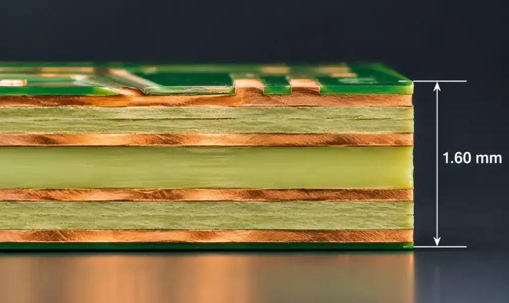
PCB thickness measures the total board height from top surface to bottom surface, including all copper layers, dielectric cores, prepreg layers, and surface finishes. Standard finished board thickness is 1.6mm (0.062 inches), established as an industry convention based on through-hole component compatibility and mechanical drilling capabilities. Modern electronics demand thicknesses from 0.4mm for ultra-thin wearables to 6.0mm for high-current power distribution systems.
Standard PCB Thickness Options
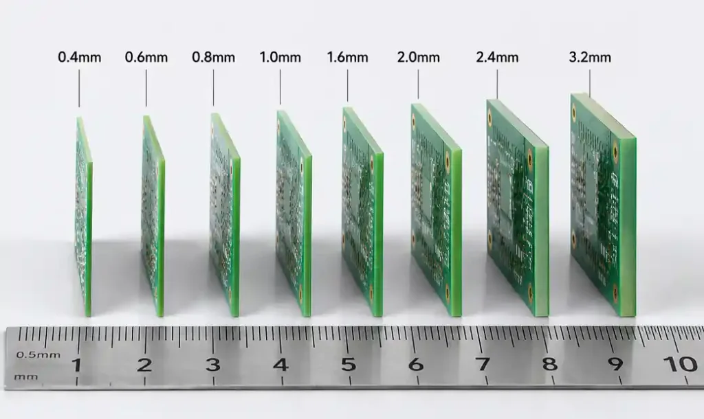
| Thickness | Imperial | Typical Applications | Aspect Ratio Limit |
|---|---|---|---|
| 0.4mm | 0.016″ | Wearables, RFID tags | 6:1 with 0.2mm drill |
| 0.6mm | 0.024″ | Smartphones, tablets | 8:1 with 0.2mm drill |
| 0.8mm | 0.031″ | Portable devices, consumer electronics | 10:1 with 0.25mm drill |
| 1.0mm | 0.039″ | Industrial handhelds, displays | 10:1 with 0.3mm drill |
| 1.2mm | 0.047″ | Telecom, medical devices | 10:1 with 0.35mm drill |
| 1.6mm | 0.062″ | General-purpose, industrial control | 10:1 with 0.4mm drill |
| 2.0mm | 0.079″ | Power electronics, motor drives | 8:1 with 0.6mm drill |
| 2.4mm | 0.093″ | High-voltage, heavy copper | 8:1 with 0.7mm drill |
| 3.2mm | 0.126″ | Power distribution, EV charging | 6:1 with 1.0mm drill |
The 1.6mm standard dominates because it provides optimal balance between mechanical rigidity, manufacturing cost, and component compatibility. This thickness supports standard through-hole components with 0.8-1.0mm lead spacing and allows 10:1 drill aspect ratio with 0.4mm minimum hole size.
Key Selection Factors
Mechanical Strength and Connector Compatibility
PCB thickness determines flexural rigidity following a cubic relationship—a 2.0mm board is 8 times stiffer than 1.0mm. Specify thicker boards when large dimensions exceed 200mm × 200mm, heavy components require support, or assemblies undergo shock and vibration per MIL-STD-810.
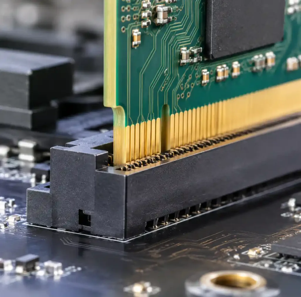
Edge connectors specify exact thickness tolerances. Standard types require:
- PCIe edge connectors: 1.6mm ±0.1mm (1.5-1.7mm)
- M.2 SSD sockets: 0.8mm ±0.05mm (0.75-0.85mm)
- Mini PCIe: 1.0mm ±0.1mm (0.9-1.1mm)
- SODIMM memory: 1.2mm ±0.1mm (1.1-1.3mm)
Thickness deviations cause intermittent contact or mechanical damage. Verify connector specifications before finalizing thickness, as custom thickness requires custom connectors with 3-5× higher cost.
Impedance Control and Stackup Design
Characteristic impedance depends on trace geometry relative to reference planes. Increasing board thickness (dielectric height) increases impedance proportionally. Standard 50Ω single-ended traces require:
| Board Thickness | Trace Width for 50Ω | Dielectric Height | Tolerance |
|---|---|---|---|
| 0.8mm | 0.2mm (8 mils) | 0.15mm | ±15% |
| 1.0mm | 0.25mm (10 mils) | 0.20mm | ±12% |
| 1.6mm | 0.35mm (14 mils) | 0.30mm | ±8% |
| 2.0mm | 0.45mm (18 mils) | 0.40mm | ±10% |
Thinner boards enable narrower traces for controlled impedance but create tighter manufacturing tolerances. For high-speed digital interfaces (USB 3.0+, PCIe Gen 3+, DDR4+), use standard 1.6mm thickness when possible. This provides mature manufacturing process control and better impedance tolerance per IPC-2141.
Drill Aspect Ratio Constraints
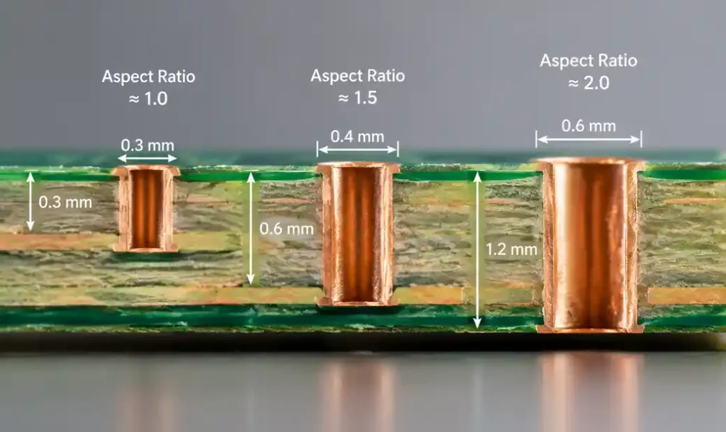
Aspect ratio defines the relationship between board thickness and minimum drill diameter:
Aspect Ratio = Board Thickness ÷ Finished Hole Diameter
Standard mechanical drilling achieves 10:1 maximum aspect ratio for reliable copper plating. Higher ratios cause plating voids and via reliability failures. Thick boards require larger minimum via sizes, reducing routing density. A 3.2mm board cannot reliably plate 0.4mm vias (13:1 ratio)—you must use 1.0mm minimum diameter. This via size limitation directly impacts HDI PCB feasibility and BGA escape routing.
Thickness Selection by Application
Ultra-Thin Boards (0.4-0.8mm)
Applications: Wearable electronics, smartphones, RFID/NFC antennas, IoT sensors
Design Considerations:
- Maximum 4-6 layers due to core thickness limits
- Often requires rigid-flex PCB construction for 0.4mm
- Surface mount only—no through-hole components
- Requires stiffeners under heavy components
- Minimum drill 0.2mm limits via density
You can achieve 0.6mm with 4-layer FR-4 using 0.1mm core plus 0.066mm prepreg. For 0.4mm, use polyimide flex or rigid-flex hybrid. These thin boards cannot survive wave soldering due to thermal shock—specify reflow-only assembly per IPC-7351.
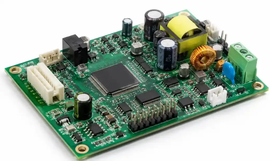
Standard Thickness Boards (1.0-1.6mm)
Applications: Consumer electronics, industrial control, telecommunications, automotive infotainment, medical devices
The 1.6mm thickness represents the industry sweet spot, supported by every PCB manufacturer worldwide with fastest lead times and lowest cost. This thickness supports 2-16 layer stackups with standard materials, achieves 10:1 aspect ratio with 0.3-0.4mm minimum via, and enables mixed SMT and through-hole assembly. For automotive applications requiring AEC-Q100 qualification, 1.6mm provides proven reliability data.
Thick Boards (2.0-3.2mm)
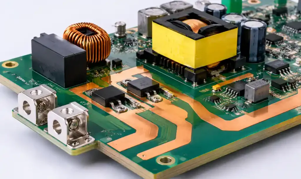
Applications: High-current power electronics, motor drives, EV charging, BMS systems
Design Considerations:
- Accommodates heavy copper up to 6oz (210μm)
- Increased current capacity—10A+ per trace
- Better thermal dissipation for power components
- Requires 0.6-1.0mm minimum via diameter
- 15-25% cost premium over 1.6mm standard
Thick boards excel at heat spreading and high-current distribution. A 2.4mm board with 4oz copper handles 15A continuous current. Specify 2.0mm+ thickness when traces carry >5A, power components dissipate >5W each, or operating voltage exceeds 100V DC.
Manufacturing Tolerances and Cost
Thickness Tolerances
IPC-6012 defines finished thickness tolerances at ±10% of nominal thickness. For 1.6mm board, Class 2 tolerance allows 1.44mm to 1.76mm (±0.16mm), though typical manufacturing achieves 1.55mm to 1.65mm (±0.05mm). Thinner boards face tighter absolute tolerances—±10% of 0.8mm is ±0.08mm, more difficult than ±0.16mm for 1.6mm boards.
Cost Structure by Thickness
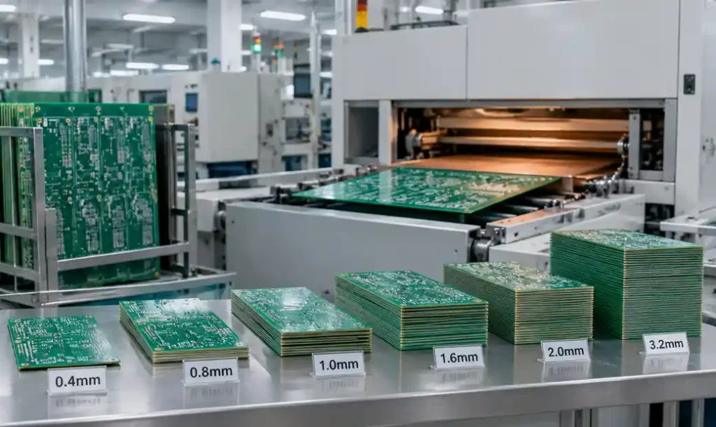
| Thickness | Relative Cost | Lead Time | Common MOQ |
|---|---|---|---|
| 0.6-0.8mm | 110-120% | 10-12 days | 100+ pcs |
| 1.0mm | 105-110% | 8-10 days | 50+ pcs |
| 1.6mm | 100% (baseline) | 7-10 days | 25+ pcs |
| 2.0mm | 115-125% | 10-12 days | 50+ pcs |
| 2.4mm | 125-140% | 12-15 days | 100+ pcs |
| 3.2mm+ | 140-180% | 15-20 days | Custom |
Standard 1.6mm thickness costs less because material is stocked by all suppliers, optimized process parameters reduce scrap rate, and higher volume throughput lowers per-unit cost.
Design Guidelines and Stackup Planning
Board thickness equals the sum of copper, core, and prepreg layers:
Total Thickness = Σ(Core) + Σ(Prepreg) + Σ(Copper Thickness)
For 1.6mm 4-layer board example:
- Outer copper: 2 × 35μm (1oz) = 70μm
- Core: 1.0mm
- Prepreg: 2 × 0.265mm = 530μm
- Total: 70μm + 1000μm + 530μm = 1600μm (1.6mm)
Use PCB stackup calculators to balance material availability with impedance requirements. Standard core thicknesses (0.1, 0.2, 0.4, 0.6, 0.8, 1.0mm) and prepreg options (1080, 2116, 7628) define achievable finished thicknesses.
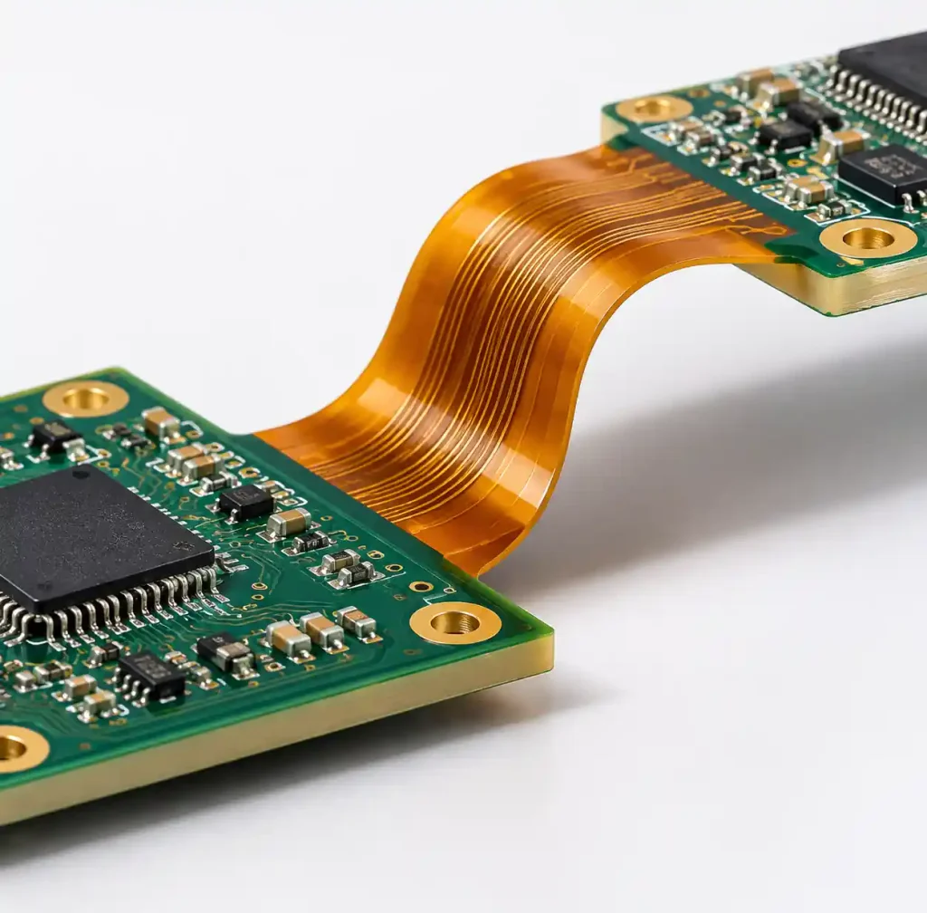
For assemblies requiring multiple thickness zones, use cavity milling (depth routing) to create thin zones or rigid-flex construction combining thin flex (0.1-0.3mm) with standard rigid zones (1.6mm).
Frequently Asked Questions
What is the most common PCB thickness?
The standard PCB thickness is 1.6mm (0.062 inches), used in 60-70% of commercial electronics. This thickness provides optimal balance between mechanical strength, manufacturing cost, and component compatibility with proven reliability per IPC-6012.
Can I use 1.0mm thickness for high-speed digital design?
Yes, but narrower traces with tighter tolerances are required. A 50Ω trace needs approximately 0.25mm width on 1.0mm board versus 0.35mm on 1.6mm board, increasing manufacturing cost 15-25% and impedance variation risk.
What minimum thickness supports heavy components?
Components exceeding 50g weight require minimum 1.6mm thickness for adequate mechanical support. For connectors with >10N insertion force or assemblies undergoing vibration testing, specify 2.0mm minimum to prevent flexural failure.
How does thickness affect cost?
Standard 1.6mm thickness is baseline cost. Thin boards (0.8mm) cost 10-20% more. Thick boards (2.4mm+) cost 25-40% more due to increased material and longer processing. Lead time increases 2-5 days for non-standard thickness.
What aspect ratio limit applies to thick boards?
Mechanical drilling achieves 10:1 maximum aspect ratio for boards up to 1.6mm thickness. Thicker boards require reduced ratio—8:1 for 2.0-2.4mm or 6:1 for 3.2mm—to ensure reliable copper plating per IPC-6012 Class 3.
Can one PCB have multiple thickness zones?
Yes, through cavity milling (depth routing) or rigid-flex construction. Cavity milling adds 25-35% cost. Rigid-flex naturally combines thin flex zones (0.1-0.3mm) with standard rigid zones (1.6mm), optimal for wearables and medical devices.
Conclusion
PCB thickness selection impacts mechanical integrity, electrical performance, and total project cost. The standard 1.6mm thickness remains optimal for most designs, providing proven reliability, fastest delivery, and lowest cost with mature process control per IPC-6012 standards. Specify thickness based on quantifiable requirements: connector mating tolerance, drill aspect ratio limits, impedance control calculations, and mechanical loading analysis. Avoid custom thickness unless measurable benefits justify 15-40% cost premium and extended lead time.
If you need PCB manufacturing with precise thickness control from 0.4mm to 6.0mm, Andwin Circuits offers advanced fabrication capabilities up to 50 layers with fast turnaround in 7 days. Our facility maintains ISO 9001, IATF 16949, and UL certification, ensuring thickness tolerances meet IPC-6012 Class 3 requirements for automotive, medical, telecommunications, and industrial applications worldwide.
Contact us today for custom PCB thickness specifications, stackup design support, and competitive factory-direct pricing.
Sources: