
Potential Defects in PCB Drilling Processes and Their Mitigation Strategies
Introduction
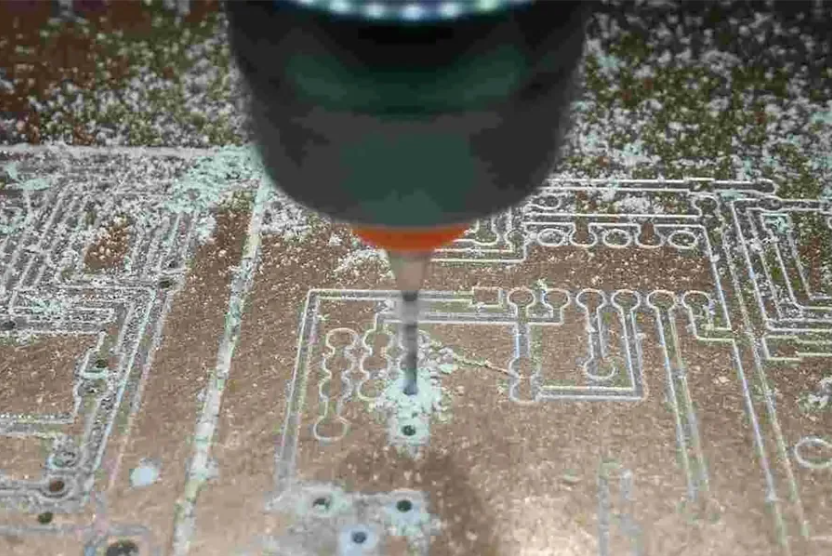
Printed Circuit Board (PCB) manufacturing involves multiple critical processes, with drilling being one of the most essential yet challenging steps. Drilling creates vias and through-holes that facilitate electrical connections between different layers of the PCB. However, due to the precision required, several defects can arise during the drilling process, affecting the board’s performance, reliability, and yield. This paper explores common defects in PCB drilling, their causes, and potential mitigation strategies.
Common Defects in PCB Drilling
1. Hole Misalignment
Description: Hole misalignment occurs when drilled holes deviate from their intended positions, leading to poor electrical connections or short circuits.
Causes:
- Inaccurate machine calibration
- Incorrect drill bit positioning
- Material movement during drilling due to insufficient clamping
- Warping of the PCB substrate
Impact: Misaligned holes can cause open circuits or unreliable interlayer connections, particularly in high-density interconnect (HDI) PCBs.
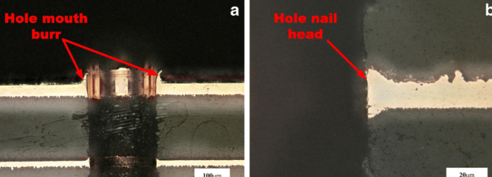
2. Burrs and Rough Hole Walls
Description: Burrs are raised edges or rough surfaces around drilled holes, which can interfere with plating and lead to poor electrical performance.
Causes:
- Dull or worn-out drill bits
- Excessive drilling speed or feed rate
- Improper drill bit geometry
Impact: Burrs can cause uneven copper plating, leading to weak interconnects or signal integrity issues.
3. Smearing and Resin Residue
Description: Smearing occurs when heat and friction during drilling cause resin from the PCB substrate to melt and smear over the hole walls, obstructing proper plating.
Causes:
- High drilling temperatures due to excessive spindle speed
- Inadequate chip evacuation (poor dust extraction)
- Use of incorrect drill parameters for the material
Impact: Resin smearing prevents proper copper deposition, leading to poor conductivity and potential via failures.
4. Nail Heading (Barrel Cracks)
Description: Nail heading refers to the widening of the hole at the entry or exit point, resembling a nail head, which can weaken the via structure.
Causes:
- Excessive drill bit wear
- Incorrect entry and exit speeds
- Poor drill bit alignment
Impact: This defect reduces mechanical strength and may cause cracks in plated through-holes (PTHs) during thermal cycling.
5. Drill Breakage
Description: Drill bits may break during the drilling process, leaving fragments in the hole or damaging the PCB.
Causes:
- Excessive feed rate or spindle speed
- Poor drill bit quality
- Hard inclusions in the PCB material (e.g., glass fibers in FR4)
Impact: Broken drill bits can cause incomplete holes, requiring rework or scrapping of the PCB.
6. Incomplete Hole Penetration
Description: Holes may not fully penetrate the PCB, leading to non-functional vias.
Causes:
- Incorrect drill depth setting
- Drill bit wear or deflection
- Uneven PCB stack-up
Impact: Incomplete holes result in open circuits, rendering the PCB unusable without rework.
7. Copper Tearing (Pad Lifting)
Description: The copper pad around a drilled hole may detach from the substrate due to mechanical stress.
Causes:
- Excessive drill bit force
- Poor adhesion between copper and substrate
- Incorrect drill entry speed
Impact: Lifted pads disrupt electrical connections and reduce PCB reliability.
8. Overheating and Thermal Damage
Description: Excessive heat generated during drilling can degrade the PCB material, leading to delamination or charring.
Causes:
- High spindle speeds without adequate cooling
- Insufficient chip removal
- Prolonged drilling time
Impact: Thermal damage weakens the PCB structure and may cause long-term reliability issues.
Mitigation Strategies
To minimize drilling defects, manufacturers should adopt the following best practices:
1. Optimize Drilling Parameters
- Adjust spindle speed and feed rate based on material type.
- Use appropriate drill bit coatings (e.g., diamond-like carbon) to reduce wear.
2. Regular Drill Bit Maintenance
- Monitor drill bit wear and replace them before excessive dulling occurs.
- Implement automated drill bit inspection systems.
3. Improve Chip Evacuation
- Use high-quality dust extraction systems to prevent resin buildup.
- Employ peck drilling (intermittent retraction) for deep holes.
4. Enhance Machine Calibration
- Regularly calibrate drilling machines to ensure positional accuracy.
- Use vision-assisted drilling systems for high-precision PCBs.
5. Material Handling Improvements
- Ensure proper PCB clamping to prevent movement during drilling.
- Use entry and exit backup materials (e.g., aluminum foil) to reduce burrs.
6. Advanced Drilling Technologies
- Implement laser drilling for microvias in HDI PCBs.
- Use automated optical inspection (AOI) to detect defects early.
Conclusion
PCB drilling is a critical yet defect-prone process that significantly impacts board reliability. Common defects such as misalignment, burrs, smearing, and drill breakage can lead to costly rework or failures in the final product. By optimizing drilling parameters, maintaining equipment, and adopting advanced technologies, manufacturers can minimize these defects and enhance PCB quality. Continuous process monitoring and defect analysis are essential for achieving high yields in modern PCB production.