
Power Integrity in PCB Design: PDN Impedance and Decoupling Strategy
Achieving target PDN impedance below 10% of load impedance across 1MHz-1GHz prevents voltage droops exceeding 5% during transient switching—the threshold where FPGA bit errors, microcontroller resets, and RF amplifier spurious emissions begin appearing in production. For a 1.0V core rail switching 10A in 50ns, this requires PDN impedance below 5mΩ, demanding strategic placement of 0.1µF-100µF capacitors, power plane spacing under 4mil, and via inductance mitigation.
If you need to design power distribution networks for high-speed digital circuits, RF power amplifiers, or any system where load current changes rapidly, then understanding PDN impedance budgeting and decoupling capacitor selection determines whether your board passes or fails EMC testing. This is not academic theory—these are the calculations and measurements we verify on every HDI PCB design before prototype release.
What is PDN Impedance and Why It Matters
PDN impedance measures the AC resistance between your voltage regulator output and the IC power pins across all switching frequencies. Unlike DC resistance (measured in ohms for power loss), PDN impedance dominates at high frequencies where inductance becomes significant.
The target impedance calculation is straightforward: Ztarget = ΔV / ΔI, where ΔV is your maximum allowable voltage ripple and ΔI is the peak current transient. For a 3.3V rail with 5% tolerance (±165mV) switching 8A, you need Ztarget = 165mV / 8A = 20.6mΩ.
This impedance must stay below target from DC to the highest switching frequency of your load—typically 10MHz for microcontrollers, 200MHz for DDR4 memory, and 1GHz for FPGAs. When PDN impedance exceeds target, voltage droop causes logic level violations, increased jitter on clock lines, and radiated emissions from di/dt transients coupling to signal traces.
PDN Impedance Contributors and Frequency Response
| Component | Frequency Range | Impedance Behavior | Mitigation Strategy |
|---|---|---|---|
| VRM output caps | DC-10kHz | ESR dominant, flat | Low-ESR electrolytics (22µF-100µF) |
| Power plane capacitance | 10kHz-10MHz | Decreasing with f | Minimize plane spacing (<4mil) |
| Ceramic decoupling | 1MHz-100MHz | Self-resonant dip | Multiple capacitor values (0.1µF, 1µF, 10µF) |
| Via & trace inductance | 100MHz-1GHz | Rising Z = j2πfL | Short traces, multiple vias per capacitor |
Bulk Capacitance: DC to 100kHz
Voltage regulators require output capacitance for stability and transient response. Typical switching regulators specify 22µF-47µF ceramic or 100µF-220µF aluminum electrolytic within 10mm of the VRM output. This bulk capacitance suppresses low-frequency ripple from the switching converter (100kHz-500kHz) and provides the initial energy reservoir during load transients.
Aluminum electrolytics have high ESR (50mΩ-200mΩ) but large capacitance, making them effective below 100kHz. Polymer electrolytics reduce ESR to 5mΩ-15mΩ while maintaining high capacitance, extending effective frequency to 500kHz.
Power Plane Capacitance: 100kHz to 10MHz
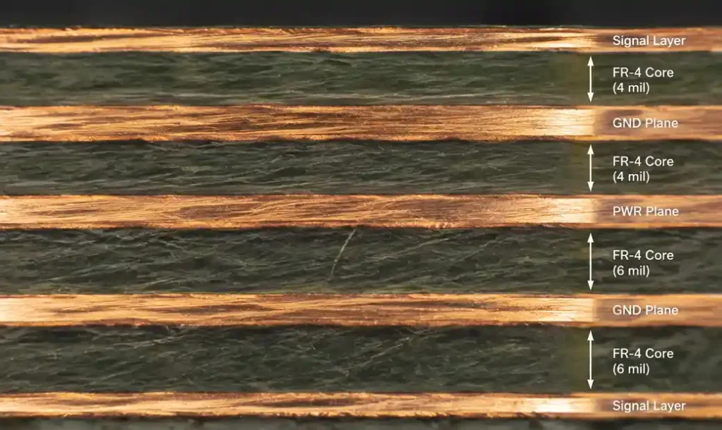
Adjacent power and ground planes separated by thin dielectric form a distributed capacitor across the entire board. For FR-4 with εr=4.3, the capacitance is C = ε₀εrA/d, yielding approximately 40pF per square centimeter with 4mil (0.1mm) spacing.
A 100mm × 100mm board with 4mil core provides 400pF plane capacitance. While small compared to discrete capacitors, plane capacitance is spatially distributed with extremely low inductance, making it highly effective in the 100kHz-10MHz range where it bridges the gap between bulk capacitors and ceramic decoupling.
Reducing plane spacing from 8mil to 4mil doubles plane capacitance and halves the self-resonant frequency of the plane pair structure, extending low-impedance performance to higher frequencies.
Decoupling Capacitor Selection and Placement Strategy
Target Impedance Method for Capacitor Sizing
Start with your target impedance Ztarget calculated from ΔV/ΔI. At the capacitor’s self-resonant frequency (SRF), its impedance reaches minimum: Z ≈ ESR. Above SRF, via and mounting inductance dominate: Z ≈ 2πfL.
For 0402 size MLCC capacitors mounted 2mm from the IC with two vias, total loop inductance is typically 0.8nH-1.2nH. At 100MHz, this creates 50mΩ-75mΩ impedance even with perfect capacitors. Therefore, meeting a 20mΩ target at 100MHz requires either larger capacitors closer to the IC or multiple parallel capacitors reducing effective inductance.
Capacitor Value Selection: The Anti-Resonance Problem
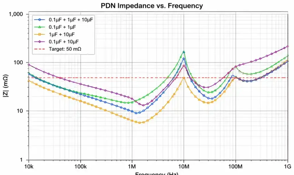
Using a single capacitor value creates an anti-resonant peak at √2 times the capacitor SRF where impedance can exceed the no-capacitor case. The solution is multi-decade capacitor spacing: typical combinations are 10µF, 1µF, and 0.1µF in ratios of 10:1.
This creates overlapping impedance profiles where each capacitor’s effective range covers the frequency gap left by adjacent values. The 10µF handles 1MHz-10MHz, the 1µF covers 10MHz-50MHz, and the 0.1µF extends to 200MHz-500MHz.
Modern FPGA designs targeting sub-5mΩ impedance use four decades: 100µF (VRM side), 10µF (regional placement), 1µF (IC side), 0.1µF (per power ball).
PDN Impedance Budgeting: From VRM to IC
| Path Segment | Inductance | Resistance | Impedance at 100MHz | Design Control |
|---|---|---|---|---|
| VRM to bulk cap | 5nH | 1mΩ | 3.1mΩ | Trace width, via count |
| Bulk cap mounting | 0.8nH | 0.2mΩ | 0.5mΩ | Pad via design |
| Power plane pair | 0.05nH/mm | 0.1mΩ/cm² | Distance dependent | Plane spacing, area |
| Decoupling cap mounting | 1.2nH | 0.3mΩ | 0.75mΩ | Via position, pad layout |
| IC package | 0.5nH/ball | 2mΩ | IC dependent | BGA selection |
Via Inductance Reduction Techniques
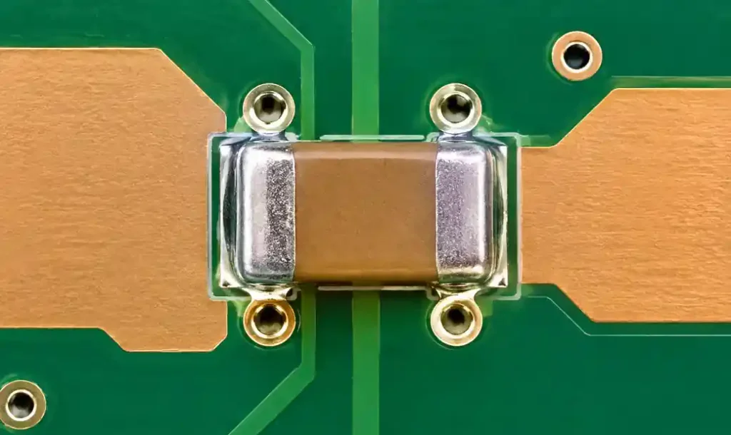
Each through-hole via contributes 1.0nH-1.5nH inductance depending on board thickness. For a 1.6mm board, a single via adds 1.2nH. Doubling vias halves inductance to 0.6nH—a 50% impedance reduction at high frequency.
Place vias immediately adjacent to capacitor pads, not at the pad edges where current must travel through the pad copper. For critical rails, use four vias per capacitor: two to power, two to ground, arranged symmetrically to balance current flow and minimize loop area.
Blind and buried vias in HDI PCB designs reduce via stub length and inductance by 30-50% compared to through-hole vias, particularly valuable for DDR4/DDR5 power delivery where 0.5nH inductance difference determines whether you meet timing margins.
Practical Decoupling Implementation for Common ICs
FPGA Power Delivery
Modern FPGAs have 4-8 power domains (core, I/O, PLL, transceiver, auxiliary) each requiring independent PDN design. Xilinx Ultrascale+ and Intel Stratix 10 specify per-rail impedance targets in their power delivery network design guides—typically 2mΩ-5mΩ for 0.85V-1.0V core rails switching 30A-50A.
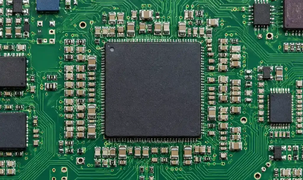
Place 1µF capacitors at every VCCINT power ball—for a 676-ball package with 120 VCCINT connections, this means 120 × 1µF capacitors in addition to 10µF bulk capacitors positioned regionally. Total capacitance often exceeds 500µF ceramic, consuming 15-25% of board area under the BGA.
Each 1µF capacitor reduces local PDN impedance by providing a low-inductance path for the specific portion of the die it serves. Die power delivery is not uniform—placing capacitors evenly across the ball array ensures all die regions have access to low-impedance power.
Microcontroller Decoupling
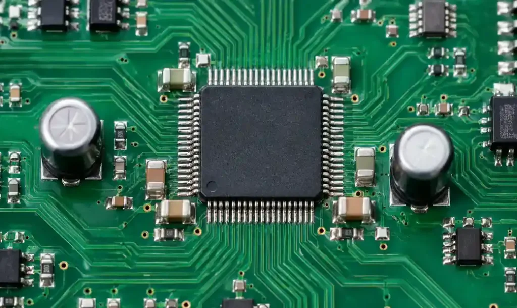
Microcontrollers typically specify one 0.1µF capacitor per power pin pair plus one 10µF bulk capacitor per voltage domain. For an STM32H7 with three power domains (VDD, VDDA, VDDUSB), you need 3 × 10µF bulk + 8 × 0.1µF local (one per VDD-VSS pair).
Place the 0.1µF capacitors within 5mm trace length of their corresponding power pins. Exceeding this distance adds 5nH-10nH inductance per 10mm, degrading effectiveness above 50MHz. For USB high-speed operation, the VDDUSB 0.1µF capacitor must be within 2mm of the USB PHY power pins to suppress switching noise that couples into the differential lines.
PDN Measurement and Verification
VNA-Based PDN Impedance Measurement
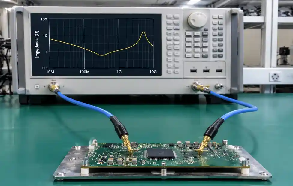
Vector network analyzers with impedance test fixtures measure PDN impedance directly by injecting current at one point and measuring voltage response at another. The Picotest PDN cable and J2154A measurement setup has become industry standard for validating PDN impedance from 10kHz to 1GHz.
Measurement requires accessing both power and ground at a test point near the IC. Some designs include dedicated measurement pads in the BGA escape routing specifically for PDN characterization. Without test points, probe-based measurement using spring-loaded probes on decoupling capacitor pads provides approximate results but adds 1-2nH probe inductance.
Comparing measured impedance to simulation validates your PDN model and confirms manufacturing execution matched design intent. Discrepancies typically trace to capacitor ESL variations, plane resonances not modeled, or via inductance higher than calculated.
Time-Domain Transient Testing
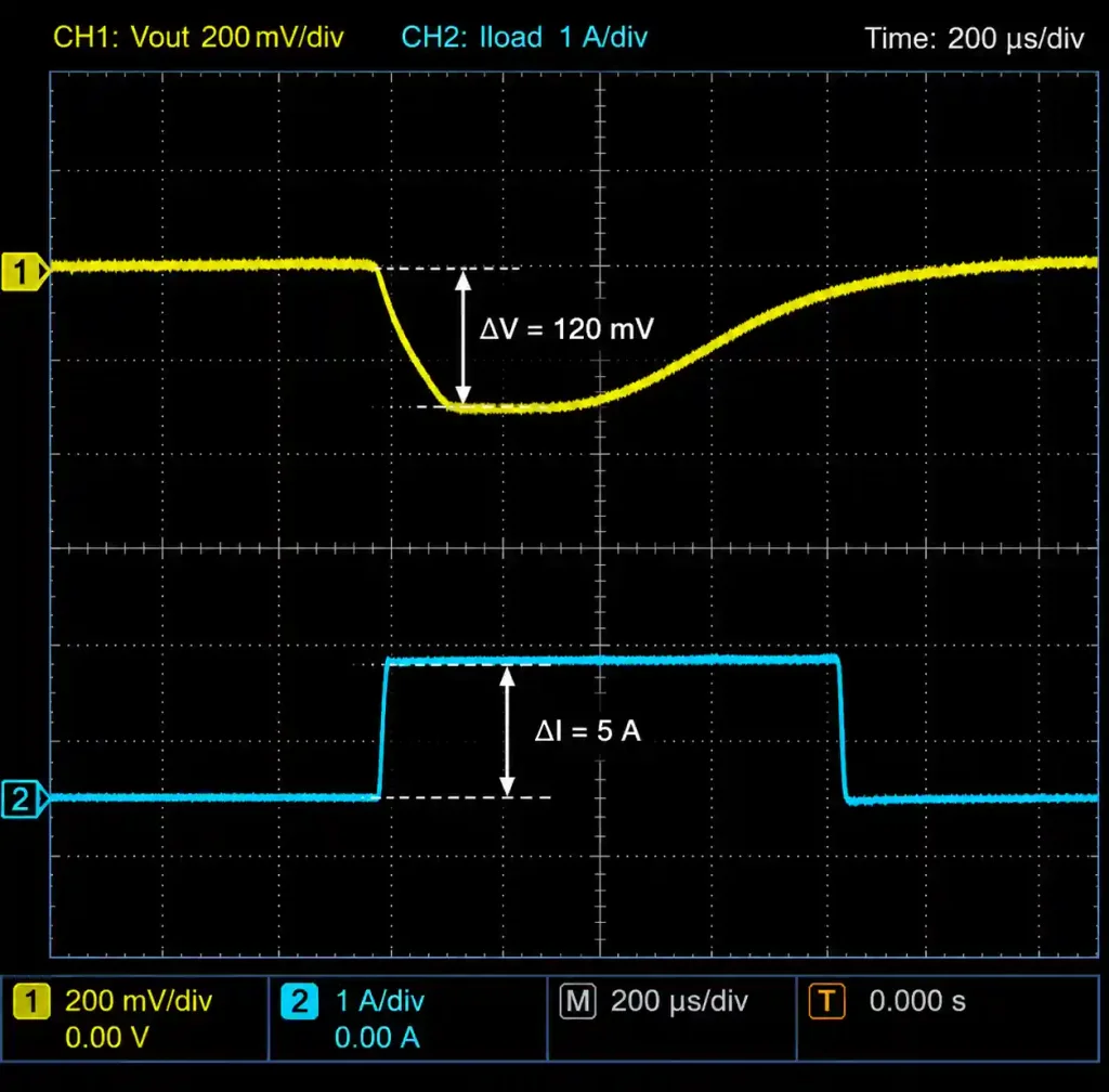
Oscilloscope-based testing measures actual voltage droop during load current steps. Apply a step load using an electronic load or pulse the IC into high-activity mode while monitoring supply voltage at IC pins with a bandwidth-adequate probe (≥1GHz for modern designs).
For a DDR4 memory buffer switching from idle (2A) to full read/write (8A) in 10ns, PDN impedance manifests as: ΔV = Z × ΔI. If measured droop is 120mV instead of calculated 40mV (assuming 5mΩ target), effective impedance is 120mV / 6A = 20mΩ—four times target, indicating inadequate decoupling or excessive via inductance.
Advanced PDN Optimization Techniques
Embedded Capacitance Materials
When ceramic capacitor count becomes prohibitive or board real estate runs out, embedded capacitance laminates offer distributed high-frequency decoupling within the PCB stack-up. Materials like 3M C-Ply achieve 5nF/cm² at 4mil thickness—50× higher than FR-4 plane pairs.
A 10cm × 10cm embedded capacitance plane provides 500nF capacitance with <100pH inductance, effective from 1MHz to 500MHz. This does not eliminate discrete capacitors but reduces the required count by 50-70%, particularly valuable in space-constrained HDI designs.
Material cost adds $2-$5 per board (prototype quantities), with volume pricing approaching standard high-Tg FR-4. Lead time increases 1-2 days for first article as fabricators confirm lamination pressure cycles.
Cavity Resonance and Via Fencing
Parallel plane pairs form cavities that resonate at frequencies where cavity dimensions equal half-wavelength. For a 150mm × 100mm board, first resonance occurs around 500MHz (λ/2 = 150mm in FR-4 with εr=4.3).
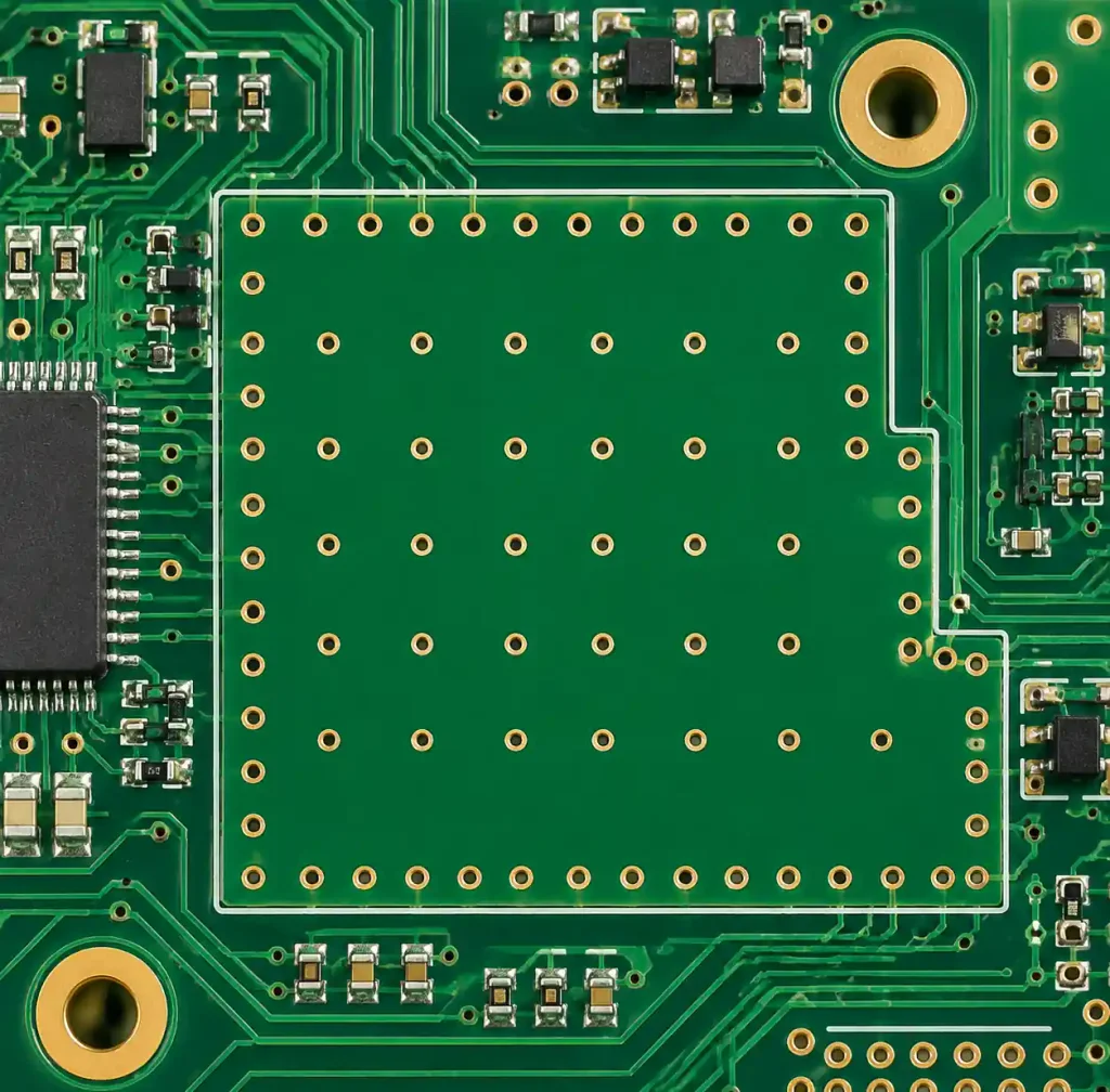
At cavity resonance, PDN impedance peaks despite adequate decoupling because standing waves concentrate current in specific board regions. Via fencing—placing grounded vias around power plane perimeters at λ/10 spacing—shorts cavity modes and suppresses resonance by 15-20dB.
For mixed-signal designs, via fencing also creates magnetic field barriers between noisy digital regions and sensitive analog sections, reducing cross-talk that would otherwise couple through the power plane structure.
FAQ
What is the difference between target impedance and actual PDN impedance?
Target impedance is the calculated maximum impedance your PDN must maintain to keep voltage droop within specification: Ztarget = ΔVallowable / ΔImax. Actual PDN impedance is measured or simulated impedance vs. frequency including all capacitors, planes, and parasitic inductances. Your design goal is keeping actual impedance below target across all frequencies where your load switches.
How many decoupling capacitors does a high-speed digital board really need?
Follow IC vendor guidelines as minimum, then verify with PDN simulation. Typical density: FPGAs require 1µF per power ball + regional 10µF every 20mm; microcontrollers need 0.1µF per power pin pair + one 10µF bulk; DDR memory modules specify 0.1µF every 25mm along the DIMM plus 10µF at each end. Total capacitor count for a mid-complexity PCB assembly board ranges from 50 to 300 capacitors.
Can I use larger capacitors instead of multiple small ones?
No. Larger capacitors have higher ESL and higher SRF, limiting their high-frequency effectiveness. A single 10µF 0805 capacitor has ~0.6nH ESL with 20MHz SRF. Ten parallel 1µF 0402 capacitors have ~0.08nH effective ESL (ten parallel paths) with 60MHz SRF. The 1µF array provides better impedance from 20MHz-200MHz where most switching noise occurs. Use large values for bulk energy storage, small values for high-frequency decoupling.
What causes the anti-resonant peak between different capacitor values?
When capacitors with different values connect in parallel, their series inductances interact with their capacitances to create an LC tank circuit. At the anti-resonant frequency, the inductive impedance of the larger capacitor equals the capacitive impedance of the smaller one, and they form a high-impedance series resonance. Proper value spacing (10:1 ratio) and sufficient component count prevents the anti-resonant peak from exceeding your target impedance.
Why do FPGAs need capacitors at every power ball but microcontrollers don’t?
FPGAs have multiple independent die regions that switch asynchronously, each drawing transient current from their nearest power connections. Package inductance prevents current sharing between distant balls—power ball 50mm from an active logic block cannot supply that block’s transient current. Microcontrollers have centralized power distribution on-die and lower total current (2A vs 50A), so one capacitor per power domain suffices.
How do I verify my PDN design before building prototypes?
Use PDN simulation tools (Ansys SIwave, Keysight ADS, Cadence Sigrity) to extract board impedance and plot Z vs. frequency. Import capacitor S-parameters from vendor models—do not use ideal capacitors. Verify impedance stays below target from DC to your highest frequency. For critical designs, order first articles with test points and measure PDN impedance with a VNA before committing to production quantities.
Conclusion
Power integrity success depends on systematic impedance budgeting from source to load, strategic capacitor selection spanning three to four decades of frequency coverage, and relentless minimization of via and trace inductance through layout discipline. Target impedance Ztarget = ΔV / ΔI must be maintained across the entire switching frequency range—using bulk capacitors below 100kHz, plane capacitance from 100kHz-10MHz, and ceramic MLCC arrays from 1MHz-1GHz. Multi-value decoupling in 10:1 ratios prevents anti-resonant peaks while ensuring each frequency decade has dedicated low-impedance paths. Via inductance reduction through multiple parallel connections and proximity placement to IC power pins determines whether your design achieves calculated target impedance or suffers 3-5× degradation in production. Verification through PDN simulation before fabrication and VNA measurement after assembly confirms your power delivery network will support reliable operation across temperature, process variation, and product lifetime.