Sink Thermal Pad MCPCB: Structure, Benefits, and Best Applications
Metal Core Printed Circuit Boards (MCPCBs) with sink thermal pads represent a critical advancement in thermal management for high-power electronics. As LED lighting, power electronics, and automotive systems demand better heat dissipation, understanding sink thermal pad MCPCB technology becomes essential for engineers and designers.
This comprehensive guide explores the structure, benefits, and optimal applications of sink thermal pad MCPCBs, helping you make informed decisions for your next high-power project.
What is a Sink Thermal Pad MCPCB?
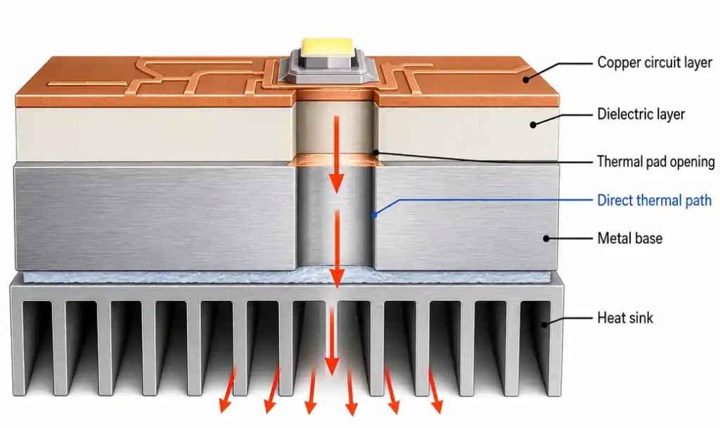
A sink thermal pad MCPCB is a specialized metal core printed circuit board featuring dedicated thermal pads that connect directly to an external heat sink. Unlike standard MCPCBs where the entire metal base acts as a heat spreader, sink thermal pad designs incorporate specific copper areas that penetrate through the dielectric layer to make direct metal-to-metal contact with the heat sink.
This direct thermal path dramatically reduces thermal resistance, allowing heat to transfer more efficiently from high-power components to the cooling system. The technology is particularly valuable in applications where component temperatures must stay within tight tolerances.
Key Characteristics
Direct Thermal Connection: Thermal pads create a low-resistance path from component to heat sink, bypassing the dielectric layer’s thermal impedance.
Selective Heat Extraction: Engineers can place thermal pads precisely where heat generation is highest, optimizing thermal management for specific components.
Mechanical Stability: The thermal pad design provides both thermal and mechanical benefits, creating robust mounting points for the PCB assembly.
Understanding MCPCB Layer Structure
To appreciate sink thermal pad technology, you need to understand the basic MCPCB construction. A standard MCPCB consists of three primary layers working together to manage heat while maintaining electrical functionality.
Standard MCPCB Layers
Copper Circuit Layer: The top layer contains the circuit traces and component pads, typically ranging from 1 oz to 10 oz copper thickness depending on current requirements.
Dielectric Insulation Layer: This thermally conductive but electrically insulating layer separates the circuit from the metal core. Modern dielectrics achieve thermal conductivity values between 1 W/m·K to 5 W/m·K.
Metal Base Layer: Usually aluminum (1-3mm thick) or copper, this layer spreads heat across the board and provides mechanical support.
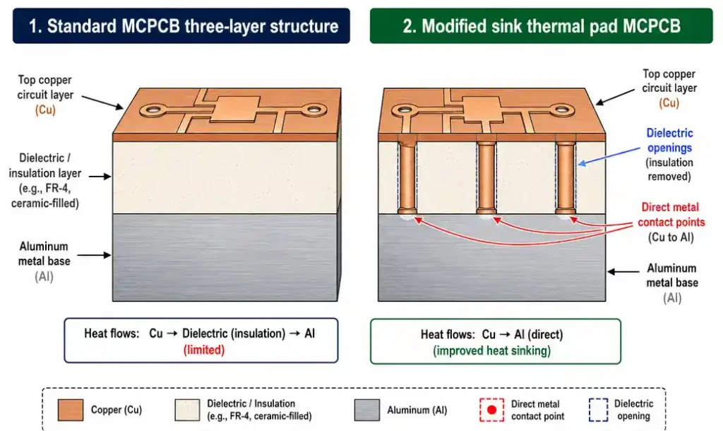
Sink Thermal Pad Modification
Sink thermal pad MCPCBs modify this structure by creating openings in the dielectric layer at strategic locations. These openings allow copper thermal pads to make direct contact with the metal base, creating thermal vias that dramatically reduce thermal resistance at critical points.
How Sink Thermal Pads Work
The thermal pad mechanism is elegantly simple yet highly effective. When a high-power component generates heat, it flows through the copper circuit layer into the thermal pad. Because the thermal pad makes direct metal-to-metal contact with the aluminum or copper base, heat transfers with minimal resistance.
Thermal Resistance Reduction
Standard MCPCB thermal resistance typically ranges from 1-3°C/W depending on dielectric thickness and thermal conductivity. Adding sink thermal pads can reduce this to 0.3-0.8°C/W at the pad locations, representing a 60-75% improvement in thermal performance.
Heat Flow Path
The optimized heat path follows this sequence: Component → Copper pad → Thermal pad → Metal base → Heat sink. Each interface is optimized to minimize thermal resistance, with thermal interface materials (TIMs) filling microscopic gaps.
Key Benefits of Sink Thermal Pad Design
Sink thermal pad MCPCBs offer multiple advantages over standard thermal management approaches, making them the preferred choice for demanding applications.
Superior Thermal Performance
The direct thermal connection reduces junction temperatures by 15-30°C compared to standard MCPCBs in high-power applications. This temperature reduction directly translates to improved component reliability and longer operational life.
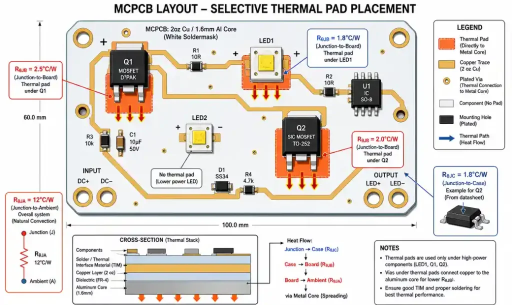
Targeted Cooling
Engineers can place thermal pads exactly where needed, allowing mixed-power designs where some components require aggressive cooling while others operate at lower power levels. This selective approach optimizes both performance and cost.
Reduced System Size
Better thermal performance means smaller heat sinks or lower airflow requirements. In space-constrained applications, this advantage enables more compact product designs without sacrificing reliability.
Improved Reliability
Lower operating temperatures reduce thermal stress on components, solder joints, and the PCB itself. This translates to longer MTBF (Mean Time Between Failures) and reduced warranty costs.
Design Flexibility
Thermal pads can be sized and positioned independently of circuit routing, giving designers more freedom to optimize both electrical and thermal performance simultaneously.
Thermal Performance Comparison
Understanding the performance differences between thermal management approaches helps justify design decisions and set realistic expectations.
Standard FR-4 PCB
Traditional FR-4 boards offer thermal conductivity around 0.3 W/m·K, making them suitable only for low-power applications. Junction temperature rise can exceed 50°C for components dissipating just 5W.
Standard MCPCB
Basic MCPCBs improve thermal conductivity to 1-2 W/m·K through the dielectric layer. This reduces temperature rise to 20-30°C for the same 5W component, a significant improvement but still limited by dielectric thermal resistance.
Sink Thermal Pad MCPCB
With direct thermal paths, sink thermal pad designs achieve effective thermal conductivity exceeding 10 W/m·K at pad locations. Temperature rise drops to 5-10°C for the same component, enabling much higher power densities.
Real-World Performance Data
In LED applications, sink thermal pad MCPCBs maintain LED junction temperatures 20-25°C cooler than standard MCPCBs under identical operating conditions. This temperature reduction can double LED lifetime while maintaining consistent light output and color temperature.
Best Applications for Sink Thermal Pad MCPCBs
Certain applications benefit dramatically from sink thermal pad technology, justifying the additional design complexity and manufacturing cost.
High-Power LED Lighting
LED arrays for automotive headlights, stadium lighting, and industrial illumination generate substantial heat in compact spaces. Sink thermal pads keep LED junction temperatures within optimal ranges, maintaining light output and preventing premature failure.
Typical Power Levels: 50-200W per board
Temperature Reduction: 20-30°C vs. standard MCPCB
Key Benefit: Extended LED lifetime and consistent color temperature
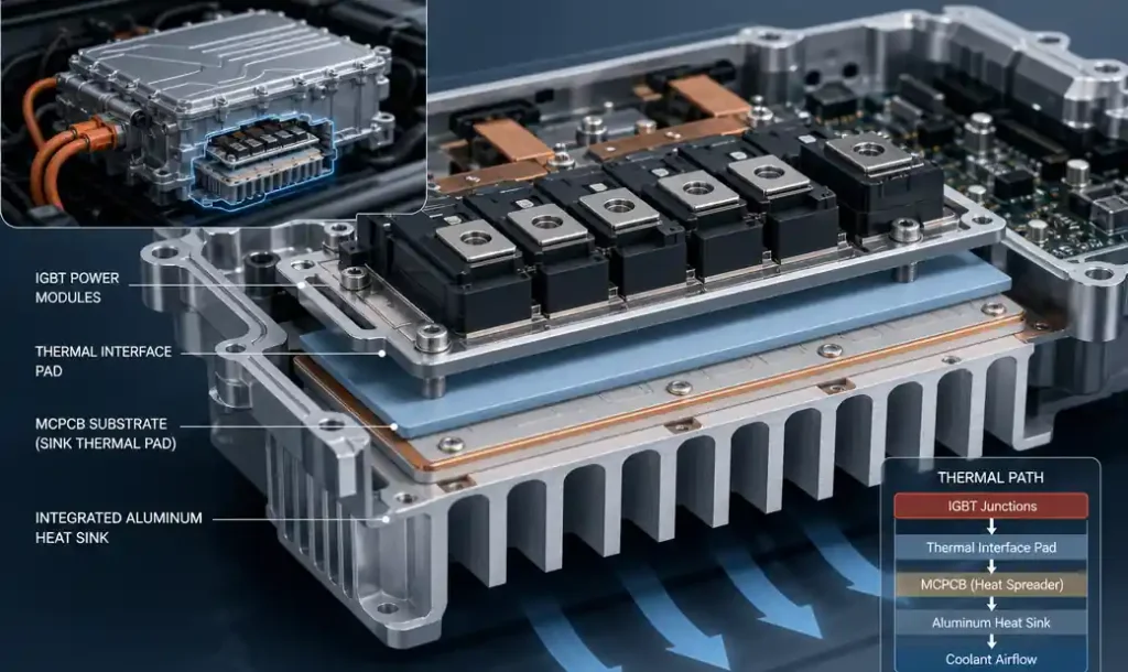
Automotive Electronics
Power modules for electric vehicles, including inverters, DC-DC converters, and battery management systems, operate in harsh thermal environments. Sink thermal pads provide the thermal performance needed for reliable operation across temperature extremes.
Typical Power Levels: 100-500W per module
Temperature Reduction: 25-40°C vs. standard MCPCB
Key Benefit: Meets automotive reliability standards (AEC-Q100)
Power Supplies and Converters
Switch-mode power supplies, especially those in compact form factors, benefit from targeted cooling of power semiconductors. Thermal pads allow higher power density without oversized heat sinks.
Typical Power Levels: 50-300W
Temperature Reduction: 15-25°C vs. standard MCPCB
Key Benefit: Smaller enclosures and reduced cooling costs
RF Power Amplifiers
High-power RF applications in telecommunications and broadcasting generate concentrated heat in power transistors. Sink thermal pads provide the thermal performance needed for stable RF output and long component life.
Typical Power Levels: 50-200W
Temperature Reduction: 20-35°C vs. standard MCPCB
Key Benefit: Stable RF performance and reduced thermal drift
Motor Drives and Controllers
Industrial motor controllers and servo drives use power MOSFETs or IGBTs that generate significant heat during switching. Thermal pads enable compact controller designs without compromising reliability.
Design Considerations and Best Practices
Successful sink thermal pad MCPCB designs require attention to both thermal and electrical requirements. Following established best practices ensures optimal performance.
Thermal Pad Sizing
Thermal pad area should match or exceed the component footprint to maximize heat transfer. For components with exposed thermal pads, the MCPCB thermal pad should extend at least 1-2mm beyond the component outline to account for assembly tolerances.
Pad Placement Strategy
Position thermal pads directly under high-power components, ensuring the thermal path is as short as possible. Avoid placing thermal pads under low-power components where the added cost provides minimal benefit.
Dielectric Thickness Selection
Thinner dielectrics (50-100μm) reduce thermal resistance but require careful attention to voltage isolation requirements. High-voltage applications may require thicker dielectrics (150-200μm), accepting slightly higher thermal resistance.
Thermal Interface Material Selection
The interface between the MCPCB metal base and heat sink critically affects overall thermal performance. Use high-quality thermal interface materials with thermal conductivity above 3 W/m·K and ensure proper application to eliminate air gaps.
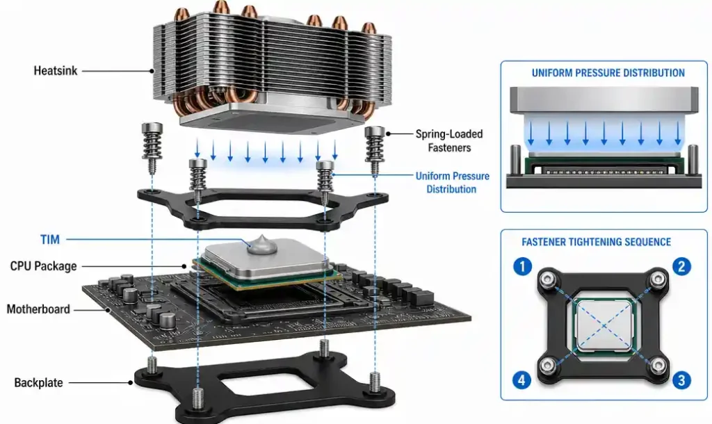
Mounting Pressure
Adequate mounting pressure ensures good thermal contact between the MCPCB and heat sink. Follow manufacturer recommendations, typically 50-100 PSI, using appropriate fastener torque specifications.
Electrical Isolation Verification
Always verify electrical isolation between the circuit layer and metal base, especially around thermal pad areas where dielectric thickness is minimal. Perform high-voltage isolation testing during prototyping.
Material Selection Guide
Material choices significantly impact thermal performance, cost, and manufacturability. Understanding the options helps optimize designs for specific requirements.
Metal Base Materials
Aluminum (5052, 6061): Most common choice, offering good thermal conductivity (150-180 W/m·K), low cost, and easy machining. Suitable for most applications.
Copper: Superior thermal conductivity (380-400 W/m·K) but higher cost and weight. Reserved for extreme thermal performance requirements.
Aluminum-Copper Composite: Balances performance and cost, using copper in high-heat areas and aluminum elsewhere.
Dielectric Materials
Standard Epoxy: Thermal conductivity 1-2 W/m·K, lowest cost, suitable for moderate power applications.
High-Performance Ceramic-Filled: Thermal conductivity 2-4 W/m·K, better performance for demanding applications.
Ultra-High Conductivity: Thermal conductivity 4-5 W/m·K, premium option for maximum thermal performance.
Copper Weight Selection
1-2 oz Copper: Standard for signal and low-current applications.
3-4 oz Copper: Better for moderate current and improved heat spreading.
5-10 oz Copper: Required for high-current applications and maximum thermal performance.
Manufacturing Process Overview
Understanding the manufacturing process helps designers create manufacturable designs and set realistic expectations for lead times and costs.
Standard MCPCB Fabrication
The process begins with preparing the metal base, typically aluminum sheet cut to panel size. The dielectric layer is applied through lamination or coating, then cured. The copper circuit layer is laminated on top, followed by standard PCB processing including imaging, etching, and solder mask application.
Thermal Pad Creation
Creating sink thermal pads requires additional process steps. The dielectric layer must be precisely removed at thermal pad locations, either through mechanical drilling, laser ablation, or selective application during lamination. The copper circuit layer is then processed to create the thermal pad features.
Quality Control
Critical inspection points include dielectric thickness measurement, thermal pad registration accuracy, and electrical isolation testing. Thermal performance testing on sample boards verifies that thermal resistance meets specifications.
Lead Times and Minimum Orders
Sink thermal pad MCPCBs typically require 2-4 weeks lead time for prototypes and 3-6 weeks for production quantities. Minimum order quantities vary by manufacturer but typically start at 5-10 pieces for prototypes and 50-100 pieces for production.
Common Design Mistakes to Avoid
Learning from common pitfalls saves time and prevents costly redesigns. These mistakes appear frequently in first-time sink thermal pad MCPCB designs.
Insufficient Thermal Pad Area
Undersized thermal pads create thermal bottlenecks that negate the benefits of the sink thermal pad design. Always size thermal pads to match or exceed component thermal pad dimensions.
Poor Heat Sink Contact
Warped boards, inadequate mounting pressure, or insufficient thermal interface material creates air gaps that dramatically increase thermal resistance. Specify flatness requirements and proper mounting procedures.
Ignoring Electrical Clearances
Thermal pads bring the metal base very close to circuit traces. Ensure adequate clearance (typically 0.5-1mm minimum) to maintain electrical isolation, especially in high-voltage designs.
Overlooking Assembly Tolerances
Component placement accuracy affects thermal pad alignment. Design thermal pads with sufficient margin to accommodate typical assembly tolerances of ±0.1-0.2mm.
Inadequate Thermal Modeling
Relying on intuition rather than thermal simulation often leads to suboptimal designs. Use thermal modeling software to verify performance before committing to fabrication.
Cost vs. Performance Analysis
Sink thermal pad MCPCBs cost more than standard MCPCBs, but the investment often pays off through improved performance and system-level savings.
Direct Cost Comparison
Standard MCPCBs typically cost $2-5 per square inch for small quantities. Sink thermal pad MCPCBs add $1-3 per square inch due to additional processing steps, bringing total cost to $3-8 per square inch.
System-Level Savings
Better thermal performance enables smaller heat sinks, reduced fan requirements, or elimination of active cooling entirely. These savings often exceed the MCPCB cost premium, especially in volume production.
Reliability Benefits
Lower operating temperatures reduce failure rates and warranty costs. For products with 3-5 year warranties, improved reliability can save significantly more than the initial MCPCB cost difference.
Break-Even Analysis
For most applications, sink thermal pad MCPCBs become cost-effective when component power dissipation exceeds 5-10W per device or when system size constraints make standard thermal management approaches impractical.
Future Trends in Thermal Management
Thermal management technology continues evolving, with several trends shaping the future of high-power PCB design.
Advanced Dielectric Materials
New dielectric formulations promise thermal conductivity exceeding 6-8 W/m·K while maintaining excellent electrical isolation. These materials will further improve MCPCB thermal performance without requiring sink thermal pads in some applications.
Embedded Cooling Channels
Research into MCPCBs with embedded microfluidic cooling channels could enable even higher power densities, though manufacturing complexity and cost remain challenges.
Hybrid Thermal Solutions
Combining sink thermal pads with heat pipes or vapor chambers creates ultra-high-performance thermal management for extreme applications like data center power supplies and electric vehicle inverters.
Additive Manufacturing
3D printing technologies may eventually enable custom thermal structures integrated directly into PCBs, allowing unprecedented design flexibility for thermal management.
AI-Driven Thermal Optimization
Machine learning algorithms are beginning to optimize thermal pad placement and sizing, potentially discovering non-intuitive designs that outperform traditional approaches.
Conclusion
Sink thermal pad MCPCBs represent a proven, cost-effective solution for high-power electronics requiring superior thermal management. By creating direct thermal paths from components to heat sinks, this technology enables higher power densities, improved reliability, and more compact designs.
The key to success lies in understanding when sink thermal pads provide sufficient value to justify their additional cost and complexity. For applications with power dissipation above 5-10W per component, operating in harsh thermal environments, or requiring maximum reliability, sink thermal pad MCPCBs deliver clear advantages.
As power densities continue increasing across LED lighting, automotive electronics, power supplies, and other applications, sink thermal pad MCPCB technology will become increasingly important. Engineers who master this technology position themselves to design the next generation of high-performance, thermally-optimized electronic systems.
Whether you’re designing your first high-power LED array or optimizing an existing power electronics design, sink thermal pad MCPCBs deserve serious consideration as part of your thermal management strategy.