6-Layer PCB Stackup Design for High-Speed Applications
Introduction In today’s rapidly advancing electronics industry, high-speed digital designs have become ubiquitous across various applications including networking equipment, telecommunications,…

Introduction In today’s rapidly advancing electronics industry, high-speed digital designs have become ubiquitous across various applications including networking equipment, telecommunications,…
Printed Circuit Boards (PCBs) are the backbone of modern electronics, providing the necessary platform for mounting and interconnecting electronic components….
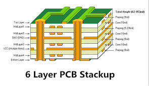
he best practices for 6-layer PCB stacking design include reasonable hierarchy, optimized signal layer layout, good power and grounding design, appropriate use of vias, and effective thermal management. By following these best practices, the performance and reliability of the circuit board can be significantly improved to meet the needs of high-performance applications.
The design and manufacturing process of 6 ayer PCB motherboard is a complex and sophisticated process involving multiple steps and technical details.
Analysis of the key steps and technical points of 6-layer PCB manufacturingThe manufacturing process of 6-layer printed circuit boards (PCBs) is complex and delicate, involving multiple key steps and technical points.
The cost analysis of 6 layer PCB cost involves multiple aspects, including materials, manufacturing and optimization strategies.
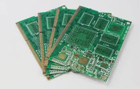
1.What is 6-layer pcb 6-layer PCB, or 6-layer printed circuit board, is a multi-layer circuit board widely used in modern…