
Telecommunication PCB Design: Backplane and High-Speed Interconnect
Telecommunication infrastructure demands PCBs that handle data rates from 10Gbps to 100Gbps while maintaining signal integrity across backplane interconnects. Backplane design accounts for 35% of signal integrity failures in telecom equipment, with impedance mismatches and crosstalk as primary culprits.
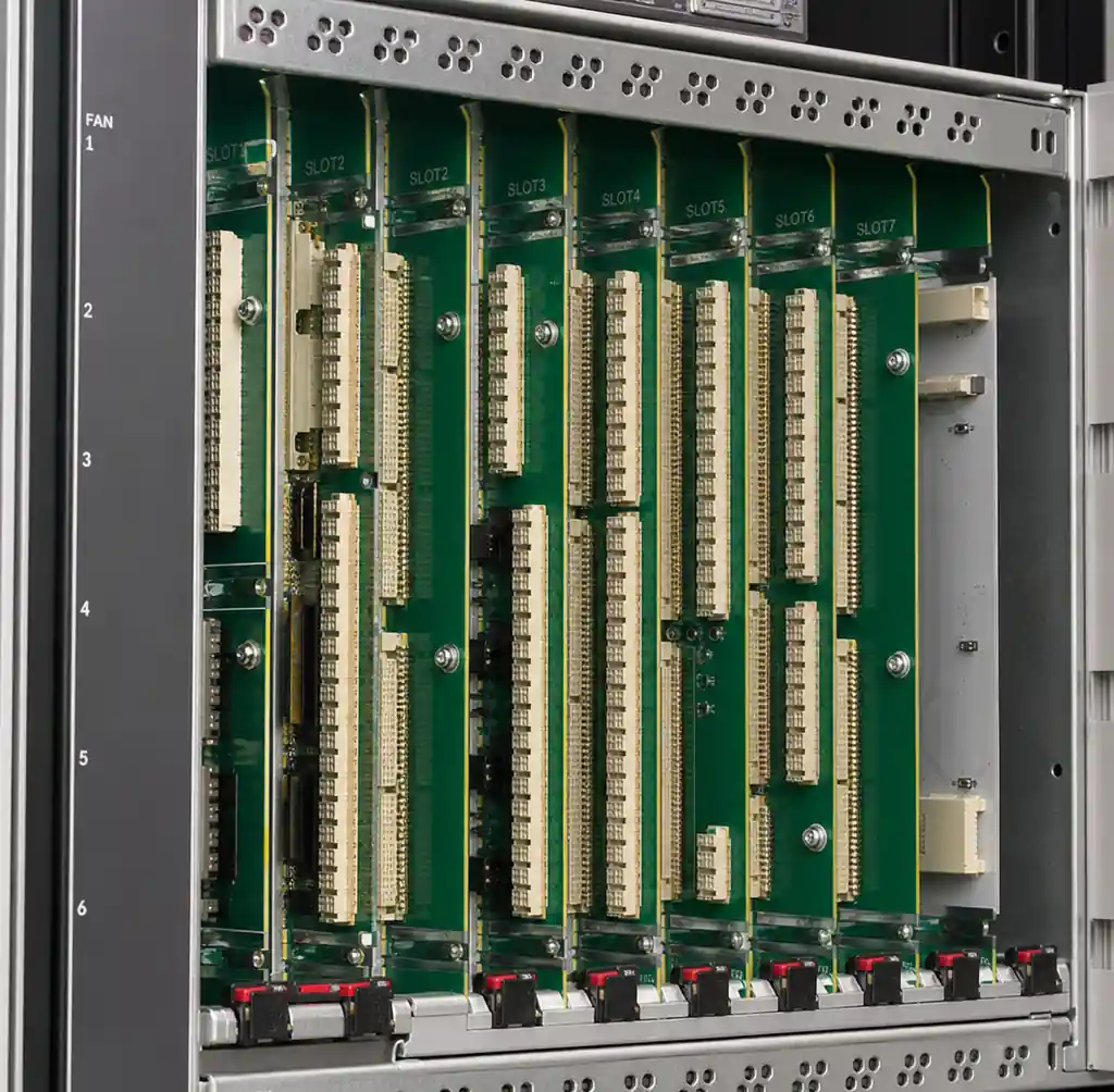
What is Telecommunication Backplane PCB?
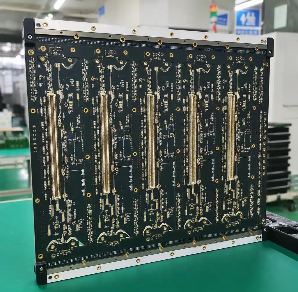
Telecommunication backplane PCB is a high-layer-count circuit board (12-30 layers) serving as the central interconnect in networking equipment, connecting line cards, switch fabrics, and I/O modules through high-speed serial links. Backplanes use specialized materials with low loss tangent (< 0.005) and controlled impedance traces to support data rates exceeding 25Gbps per lane.
High-speed serial standards like PCIe Gen4 (16GT/s), 100G Ethernet, and OIF-CEI protocols require precise impedance control of 85Ω or 100Ω differential pairs with ±10% tolerance. According to IPC-2141A, trace length matching must be within 5-10 mils for differential pairs operating above 10Gbps.
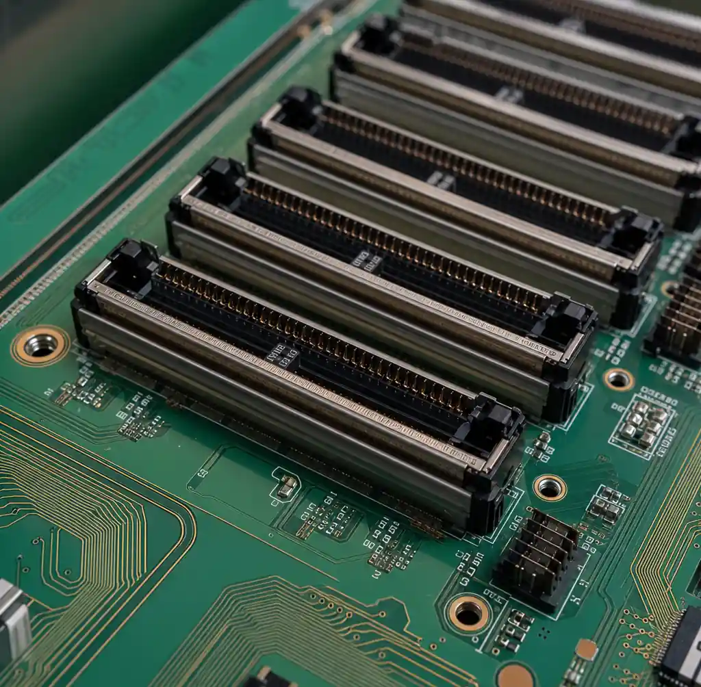
Backplane Architecture Types
Passive Backplane
Passive backplanes contain only copper traces and connectors with no active components. This offers flexibility and easier maintenance since intelligence resides on replaceable line cards. Trace length ranges from 10-20 inches, requiring careful impedance control. Testing per IPC-TM-650 shows FR4 (Dk 3.8-4.2) supports 10Gbps over 15 inches, while 25Gbps needs low-loss materials like Megtron 6 (Dk 3.6, Df 0.004).
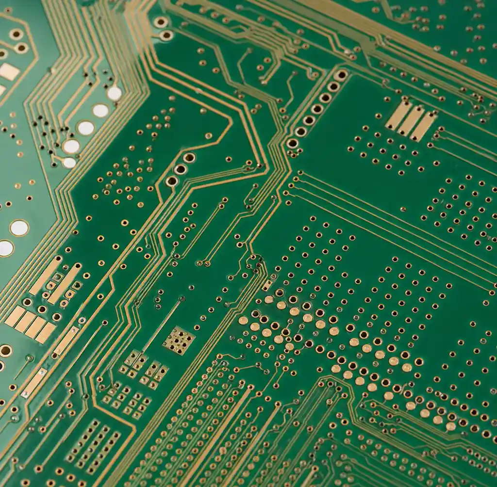
Active Backplane
Active backplanes integrate signal re-drivers or retimers directly on the backplane to regenerate signals. This extends reach and supports higher data rates but increases complexity. Choose active backplanes for systems exceeding 25Gbps per lane or when traces exceed 18 inches. Active backplanes consume 40-60W additional power but enable 100Gbps link speeds.
High-Speed Serial Standards Comparison
| Standard | Data Rate | Differential Impedance | Trace Length | Material Requirement |
|---|---|---|---|---|
| PCIe Gen3 | 8GT/s | 85Ω ±10% | Up to 20 inches | Standard FR4 |
| PCIe Gen4 | 16GT/s | 85Ω ±7% | Up to 15 inches | Low-loss (Df<0.005) |
| 100G Ethernet | 25Gbps/lane | 100Ω ±10% | 10-12 inches | Very low-loss (Df<0.004) |
| OIF-CEI 28G | 28Gbps | 100Ω ±10% | 8-10 inches | Ultra low-loss (Df<0.003) |
Signal Integrity Design
Controlled impedance is critical above 5Gbps. IPC-2141A specifies ±10% tolerance for 10Gbps and ±7% for 25Gbps. For 100Ω differential impedance, typical geometry uses 5mil trace width with 6mil spacing on 5mil dielectric (Dk 3.8).
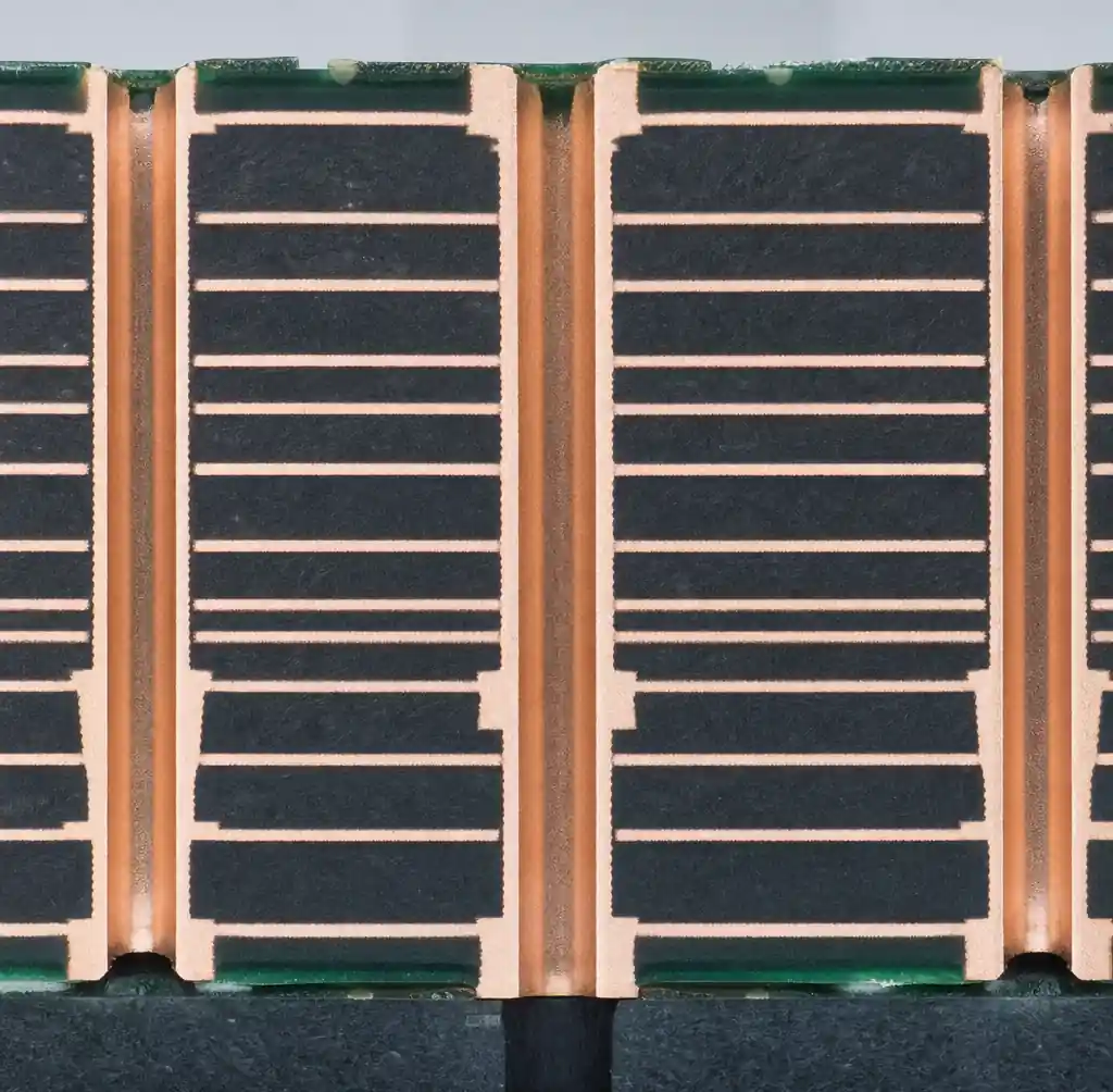
Via stubs create impedance discontinuities. For 25Gbps, minimize stub length under 10 mils through back-drilling or blind vias. A 25mil stub reduces eye height by 30% at 25Gbps.
Differential pairs need tight coupling and length matching. Match lengths to 5 mils for 10Gbps and 3 mils for 25Gbps. Avoid reference plane changes or use stitching vias within 50 mils.
PCB Material Selection
| Material | Dk @ 10GHz | Df @ 10GHz | Max Data Rate | Cost Factor |
|---|---|---|---|---|
| Standard FR4 | 4.2-4.5 | 0.018-0.025 | 5-8Gbps | 1.0x |
| Mid-Loss FR4 | 3.9-4.2 | 0.008-0.012 | 10Gbps | 1.3x |
| Low-Loss (Megtron 6) | 3.6 | 0.004 | 25Gbps | 2.0x |
| Ultra Low-Loss (Rogers) | 3.5 | 0.0027 | 56Gbps+ | 3.5x |
Standard FR4 exhibits 0.5-0.8dB/inch loss at 10GHz, while low-loss materials reduce loss to 0.15-0.25dB/inch. Specify low-loss materials for traces exceeding 10 inches at 10Gbps+.
Power Distribution and Thermal Management
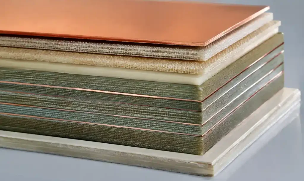
Telecom backplanes deliver 100-300W per slot. PDN impedance should remain below 10mΩ from DC to 100MHz. Use 3oz copper on power layers to reduce DC resistance by 50% versus 1oz.
Effective decoupling requires bulk capacitors (100-470μF), ceramic (10μF-100nF), and small 0201-size (100pF-10nF) within 2mm of power pins.
Backplanes dissipate 50-150W through copper traces. 3oz copper reduces operating temperature by 20-25°C versus 1oz. For extreme power, consider metal core PCB with 1-3 W/mK thermal conductivity.
Connector Selection and EMI Containment
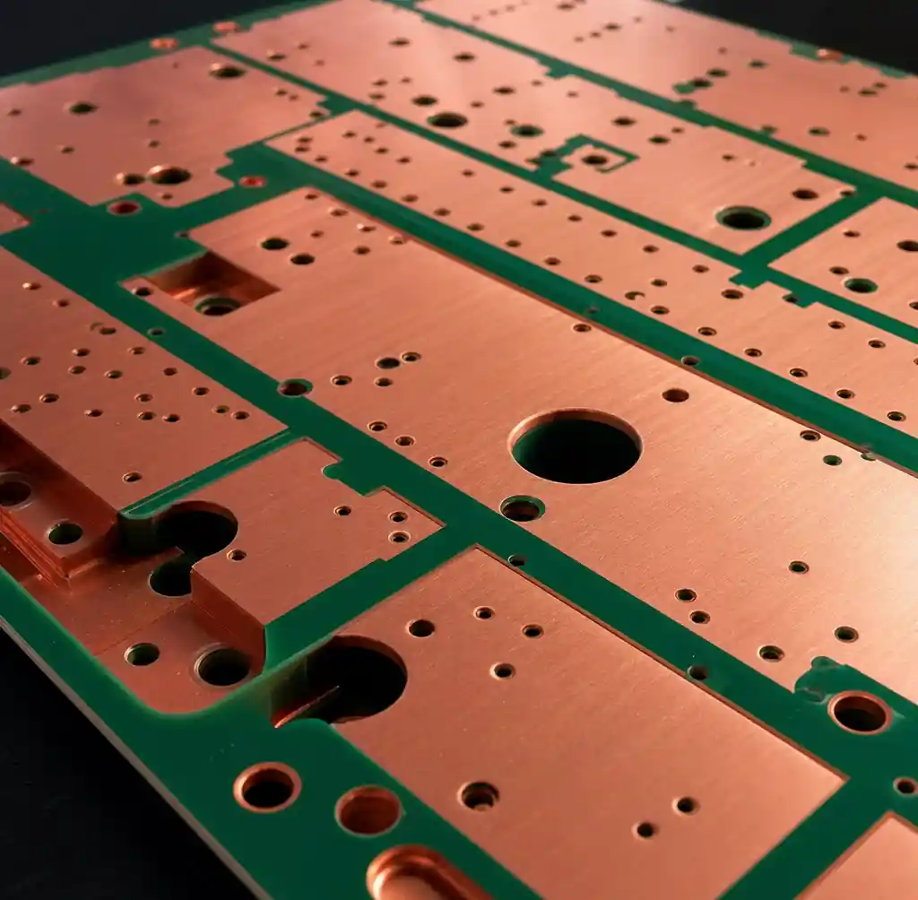
Specify connectors designed for target data rates with proven insertion loss and crosstalk performance. Common telecom backplane connectors include VITA 46 (VPX), AdvancedTCA, and Samtec high-speed orthogonal connectors supporting 25-56Gbps per differential pair.
High-current power delivery requires connectors rated for 6-10A per pin with appropriate derating. Power connector pin count should provide 50% margin above maximum current.
Ground planes provide shielding effectiveness of 40-60dB. Avoid slots or splits in ground planes beneath high-speed traces. Bridge plane splits with stitching capacitors (100nF-1nF) within 200 mils of crossing traces.
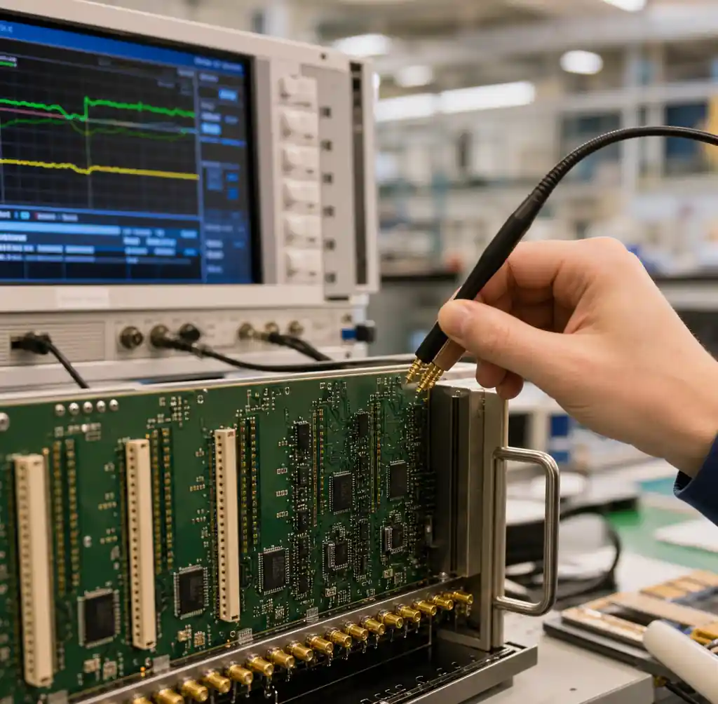
Specify PCB E-test per IPC-TM-650 to verify continuity, isolation, and impedance before assembly.
Layer Stackup Example
For 16-layer telecom backplane supporting 25Gbps:
- Layers 1, 16: High-speed signal
- Layers 2, 15: Ground planes
- Layers 3, 14: High-speed signal
- Layers 4, 13: Ground planes
- Layers 5, 12: Power planes (3.3V, 12V)
- Layers 6, 11: Ground planes
- Layers 7, 10: Low-speed signal
- Layers 8, 9: Power planes (5V, 48V) with 3oz copper
This stackup provides excellent shielding, low PDN impedance, and routing flexibility. Total thickness approximately 0.126 inches (3.2mm).
Andwin Circuits specializes in HDI PCB and multilayer stackup design with up to 50-layer capability and fast turnaround in 7 days.
FAQ
What data rates can standard FR4 support in backplane designs?
Standard FR4 materials reliably support data rates up to 8-10Gbps for trace lengths under 15 inches. Beyond 10Gbps, specify low-loss materials with loss tangent below 0.005.
How many layers are required for telecom backplane PCBs?
Typical telecom backplanes require 12-20 layers for high-speed signal routing, multiple power networks, and shielding. Complex systems may require 24-30 layers depending on port density and data rates.
What impedance tolerance is acceptable for 25Gbps differential pairs?
For 25Gbps signaling, specify differential impedance tolerance of ±7% or tighter (e.g., 100Ω ±7Ω). Manufacturing within ±5Ω is achievable through careful stackup design and testing per IPC-TM-650.
Should I use back-drilling for via stub reduction?
Back-drilling is recommended for all vias on signal paths operating above 15Gbps. Cost increase is 10-15% but provides significant signal integrity improvement.
What copper weight should I specify for backplane power planes?
For line cards drawing 100-200W per slot, specify 3oz (105μm) copper on power distribution layers. This balances DC resistance, current capacity, and cost.
Conclusion
Telecommunication PCB design for backplanes and high-speed interconnects requires expertise in signal integrity, power distribution, thermal management, and telecom-grade reliability standards. Key considerations include controlled impedance with ±7-10% tolerance for data rates above 10Gbps, low-loss materials for traces exceeding 10 inches, proper via stub management, robust power distribution with 3oz+ copper planes, and comprehensive EMI containment.
If you need high-quality telecommunication backplane PCBs for 5G infrastructure, network switching equipment, or optical transport systems, Andwin Circuits offers advanced manufacturing capabilities up to 50 layers with fast turnaround in 7 days. Our facility is certified to ISO 9001 and IATF 16949 standards.
Contact us today for custom telecom PCB solutions and competitive factory-direct pricing.