An introduction to the principles of PCB design for improved EMC
Nowadays, as the trend increases, most of the automotive, consumer and industrial applications usually contain one or more microcontrollers. Usually several electronic modules build an application system, although several applications and/or systems may run nearby. As the number of electronic applications increases, their density in any given environment increases. Therefore, the ambient electromagnetic noise observed at a given location over a long period of time increases, as shown in curve 1 in Figure 1 below. As long as the electronic device’s immunity at any given point in time is higher than the ambient electromagnetic noise, its functionality will not be affected.
First, the foundation of good EMC design is the application of good electrical and mechanical design principles. These include reliability considerations such as meeting design specifications within acceptable tolerances, good assembly practices, and various testing techniques being developed.
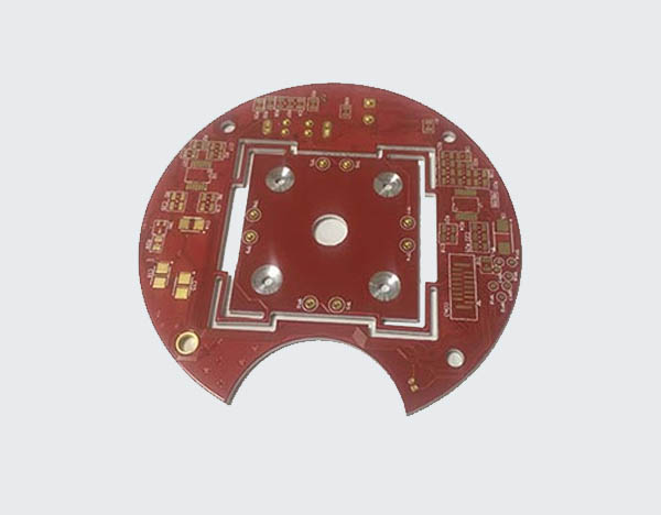
Typically, the devices that drive today’s electronic equipment are mounted on PCBs. These devices consist of components and circuits that are potential sources of interference and are sensitive to electromagnetic energy. Therefore, EMC design of PCB is the next most important issue in EMC design. The location of active components, the routing of printed lines, impedance matching, grounding design and circuit filtering should all be considered during EMC design. Some PCB components also require shielding.
Based on the requirement, heavy copper PCBs can be expensive to produce.Thus, it is more complex in design but more effective in producing heavy copper PCB.
Third, internal cables are typically used to connect PCBs or other internal subcomponents. Therefore, internal cable EMC design including routing methods and shielding is very important to the overall EMC of any given device.Copper core PCB is a copper substrate + Insulated layer + copper,can well meet the needs of this design

Long-term environmental noise development
It is obvious that if the intersection point P is reached, the entire electronic market will collapse. Therefore, the electronics market must take steps to improve the electromagnetic compatibility (EMC) of electronic systems, thereby continuously pushing point P toward infinity on the timeline.
From the perspective of EMC (electromagnetic compatibility) design, the EMC design of the PCB board is the basis of the EMC system design. The initial stage of PCB board EMC design is the setting of layers. Unreasonable layer design may produce a lot of noise and cause EMI interference and its own EMC problems. Therefore, reasonable layer layout is as important as circuit design.
To make the layer layout of the PCB system meet its electromagnetic compatibility requirements, the system layer layout usually needs to start from three points: the corresponding functional module distribution; the performance index requirements of the comprehensive single board; and the cost affordability. The PCB board layer is composed of power layer, ground layer and signal layer. The selection of layers, the relative positions of layers, and the division and distribution of power and ground planes will play a vital role in the wiring of the PCB board, signal quality, interface circuit processing, and the EMC index of the single board, and will also directly affect the entire machine. Electromagnetic compatibility of equipment.A well designed high frequency PCB ( printed circuit board RF PCB) can provide a significant boost,As the RF PCB can improve a product’s performance, stability and reliability.