PCB circuit board production process
The production process of PCB (Printed Circuit Board) can be roughly divided into the following steps:
Open material. First, cut the copper-clad laminate (a fiberglass or epoxy material covered with a copper film on both sides) to the desired size. Copper clad laminate is the basic material of PCB and is used to fix electronic components and provide paths for circuit connections.
drilling. Position the copper-clad board according to the design drawing, and use a drill to accurately drill holes. These holes are used to insert the pins of electronic components. 2345
Inner layer production. Pattern transfer (such as using dry film or film) is performed on the inner copper-clad board, followed by chemical treatment (such as copper plating) and graphic plating (such as copper plating and tin plating) to form the base layer of the circuit.
laminated. The inner copper-clad laminate and the prefabricated outer copper-clad laminate (if any) are laminated together in a specific order to form a multi-layer PCB. 14
Drilling and cladding. Repeat steps such as drilling, pattern transfer, and electroplating on the outer copper-clad board to form the final circuit layer.
etching. Use a chemical etching solution to remove the non-circuit portions of the copper layer so that a circuit pattern can be formed on the copper layer. 1234
Surface treatment. Perform surface treatment on the PCB, such as spray tin, immersion gold, etc., to protect the circuit and prevent tin from the circuit when soldering parts. twenty three
Forming and testing. Cut and trim the PCB to ensure that its dimensions meet the requirements. Then conduct tests to check whether there are defects such as short circuits and open circuits.
Final inspection. Conduct a comprehensive inspection of the PCB’s appearance, size, hole diameter, board thickness, markings, etc. to ensure that it meets quality standards.
This process may vary based on specific product requirements and design criteria, but the basic steps are similar.
What are the process flows of PCB board making? PCB circuit boards are used in almost all electronic products, ranging from watches and headphones to military and aerospace industries, which are all inseparable from the application of PCB. Although it is widely used, most people do not Now that we know how PCB is produced, let’s take a look at the manufacturing process and production process of PCB!
The PCB board making process can be roughly divided into the following twelve steps. Each process requires multiple processes. It should be noted that boards with different structures have different process flows. The following process is the complete production of multi-layer PCB. process flow;
1. Inner layer; mainly used to make the inner circuit of the PCB circuit board; the production process is:
1. Cutting: Cut the PCB substrate into production size;
2. Pretreatment: Clean the surface of the PCB substrate and remove surface contaminants
3. Lamination: stick the dry film on the surface of the PCB substrate to prepare for subsequent image transfer;
4. Exposure: Use exposure equipment to expose the coated substrate with ultraviolet light, thereby transferring the image of the substrate to the dry film;
5. DE: The exposed substrate will be developed, etched, and film removed to complete the production of the inner layer board.
2. Internal inspection; mainly for testing and repairing board circuits;
1. AOI: AOI optical scanning can compare the image of the PCB board with the data of the good quality board that has been entered to find defects such as gaps and depressions in the board image;
2. VRS: The bad image data detected by AOI is transmitted to VRS and repaired by relevant personnel.
3. Repair the wire: Solder the gold wire to the gap or depression to prevent electrical failure;
3. Lamination; as the name suggests, multiple inner layers are pressed into one board;
1. Browning: Browning can increase the adhesion between the board and the resin and increase the wettability of the copper surface;
2. Riveting: Cut the PP into small sheets and normal size so that the inner layer board is combined with the corresponding PP.
3. Lamination, target shooting, edging, and edging;
4. Drilling: Use a drilling machine to drill holes of different diameters and sizes on the board according to the customer’s requirements, so that there are holes between the boards for subsequent processing of plug-ins, and it can also help the board to dissipate heat;
5. Primary copper plating: Copper plating the drilled holes on the outer layer board to make the circuits on each layer of the board conductive;
1. Deburring line: remove burrs around the board holes to prevent poor copper plating;
2. Glue removal line: remove the glue residue inside the hole to increase adhesion during micro-etching;
3. One copper (pth): Copper plating in the hole makes the circuits on each layer of the board conductive and increases the copper thickness;
6. Outer layer; The outer layer process is roughly the same as the inner layer in the first step, and its purpose is to facilitate the subsequent process to make the circuit;
1. Pre-treatment: Clean the board surface through pickling, grinding and drying to increase dry film adhesion;
2. Lamination: stick the dry film on the surface of the PCB substrate to prepare for subsequent image transfer;
3. Exposure: irradiate with UV light to make the dry film on the board form a polymerized and unpolymerized state;
4. Development: Dissolve the dry film that has not polymerized during the exposure process, leaving a gap;
7. Secondary copper and etching; secondary copper plating and etching;
1. Second copper: electroplating pattern, applying chemical copper to the areas in the holes that are not covered by dry film; at the same time, further increasing the conductivity and copper thickness, and then tin plating to protect the integrity of the lines and holes during etching;
2. SES: Etch the bottom copper in the attachment area of the outer dry film (wet film) through film removal, etching, tin stripping and other processes, and the outer circuit is now completed;
8. Solder mask: It can protect the board and prevent oxidation and other phenomena;
1. Pre-treatment: Perform pickling, ultrasonic washing and other processes to remove oxides from the board and increase the roughness of the copper surface;
2. Printing: Cover the areas of the PCB board that do not need to be soldered with solder resist ink to protect and insulate;
3. Pre-baking: dry the solvent in the solder mask ink and harden the ink for exposure;
4. Exposure: The solder mask ink is cured by UV light irradiation, and a high molecular polymer is formed through photosensitive polymerization;
5. Development: remove the sodium carbonate solution in the unpolymerized ink;
6. Post-baking: completely harden the ink;
9. Text; printed text;
1. Pickling: Clean the surface of the board and remove surface oxidation to enhance the adhesion of printing ink;
2. Text: printed text to facilitate subsequent welding processes;
10. Surface treatment OSP; the side of the bare copper plate to be welded is coated to form an organic film to prevent rust and oxidation;
11. Molding: Get the board shape required by the customer to facilitate the customer’s SMT patching and assembly;
12. Flying probe test; test the board circuit to avoid short-circuit board leakage;
13. FQC; final inspection, sampling and full inspection after completion of all processes;
14. Packaging and shipment; vacuum-pack the completed PCB boards, pack them for shipment, and complete the delivery;
PCB circuit board is an indispensable part of electronic products. It is the carrier of electronic components. Through the connection between the wires and components on the circuit board, various functions of electronic products are realized. In the design and manufacturing process of electronic products, the production of PCB circuit boards is a very important part. Next, let’s take a closer look at the PCB circuit board production process.
Edit Image Search
1. Design circuit schematic diagram
First, the circuit schematic diagram needs to be designed according to the functional requirements of the electronic product. The circuit schematic diagram is the basis of circuit design. It describes the connection relationship between various components in the circuit and the working principle of the circuit.
2. PCB layout design
Based on the circuit schematic diagram, PCB layout design needs to be carried out. PCB layout design is the process of arranging the components and wires in the circuit schematic diagram on the PCB circuit board. In layout design, factors such as the distance between components, the length and direction of wires, and the size of the circuit board need to be considered to ensure the stability and reliability of the circuit board.
3. PCB circuit board production
PCB circuit board fabrication is the process of converting PCB layout design into actual circuit board. The production process includes the following steps:
(1) Make a printed circuit board (PCB): Print the PCB layout design onto a transparent film, then place the transparent film on a copper plate for exposure and corrosion, and finally obtain the PCB circuit board.
(2) Drilling: Drill holes on the PCB circuit board to install components and connect wires.
(3) Place components: Paste the components onto the PCB circuit board according to the position on the PCB layout design drawing.
(4) Welding: Connect components and wires through welding to form a circuit.
Edit Image Search
4. Testing and Debugging
After completing the production of the PCB circuit board, testing and debugging are required to ensure the normal operation of the circuit board. Testing and debugging include the following steps:
(1) Check whether the components and wires on the circuit board are connected correctly.
(2) Use testing instruments to test the circuit board and check whether the various indicators of the circuit board meet the requirements.
(3) Debugging the circuit and adjusting circuit parameters to ensure the normal operation of the circuit board.
Through the above steps, the production of PCB circuit board is completed. The production process of PCB circuit boards needs to be operated in strict accordance with standards to ensure the stability and reliability of the circuit board.
The production process of PCB (Printed Circuit Board) can be roughly divided into the following steps:
Open material. First, cut the copper-clad laminate (a fiberglass or epoxy material covered with a copper film on both sides) to the desired size. Copper clad laminate is the basic material of PCB and is used to fix electronic components and provide paths for circuit connections.
drilling. Position the copper-clad board according to the design drawing, and use a drill to accurately drill holes. These holes are used to insert the pins of electronic components. 2345
Inner layer production. Pattern transfer (such as using dry film or film) is performed on the inner copper-clad board, followed by chemical treatment (such as copper plating) and graphic plating (such as copper plating and tin plating) to form the base layer of the circuit.
laminated. The inner copper-clad laminate and the prefabricated outer copper-clad laminate (if any) are laminated together in a specific order to form a multi-layer PCB. 14
Drilling and cladding. Repeat steps such as drilling, pattern transfer, and electroplating on the outer copper-clad board to form the final circuit layer.
etching. Use a chemical etching solution to remove the non-circuit portions of the copper layer so that a circuit pattern can be formed on the copper layer. 1234
Surface treatment. Perform surface treatment on the PCB, such as spray tin, immersion gold, etc., to protect the circuit and prevent tin from the circuit when soldering parts. twenty three
Forming and testing. Cut and trim the PCB to ensure that its dimensions meet the requirements. Then conduct tests to check whether there are defects such as short circuits and open circuits.
Final inspection. Conduct a comprehensive inspection of the PCB’s appearance, size, hole diameter, board thickness, markings, etc. to ensure that it meets quality standards.
This process may vary based on specific product requirements and design criteria, but the basic steps are similar.
What are the process flows of PCB board making? PCB circuit boards are used in almost all electronic products, ranging from watches and headphones to military and aerospace industries, which are all inseparable from the application of PCB. Although it is widely used, most people do not Now that we know how PCB is produced, let’s take a look at the manufacturing process and production process of PCB!
The PCB board making process can be roughly divided into the following twelve steps. Each process requires multiple processes. It should be noted that boards with different structures have different process flows. The following process is the complete production of multi-layer PCB. process flow;
1. Inner layer; mainly used to make the inner circuit of the PCB circuit board; the production process is:
1. Cutting: Cut the PCB substrate into production size;
2. Pretreatment: Clean the surface of the PCB substrate and remove surface contaminants
3. Lamination: stick the dry film on the surface of the PCB substrate to prepare for subsequent image transfer;
4. Exposure: Use exposure equipment to expose the coated substrate with ultraviolet light, thereby transferring the image of the substrate to the dry film;
5. DE: The exposed substrate will be developed, etched, and film removed to complete the production of the inner layer board.
2. Internal inspection; mainly for testing and repairing board circuits;
1. AOI: AOI optical scanning can compare the image of the PCB board with the data of the good quality board that has been entered to find defects such as gaps and depressions in the board image;
2. VRS: The bad image data detected by AOI is transmitted to VRS and repaired by relevant personnel.
3. Repair the wire: Solder the gold wire to the gap or depression to prevent electrical failure;
3. Lamination; as the name suggests, multiple inner layers are pressed into one board;
1. Browning: Browning can increase the adhesion between the board and the resin and increase the wettability of the copper surface;
2. Riveting: Cut the PP into small sheets and normal size so that the inner layer board is combined with the corresponding PP.
3. Lamination, target shooting, edging, and edging;
4. Drilling: Use a drilling machine to drill holes of different diameters and sizes on the board according to the customer’s requirements, so that there are holes between the boards for subsequent processing of plug-ins, and it can also help the board to dissipate heat;
5. Primary copper plating: Copper plating the drilled holes on the outer layer board to make the circuits on each layer of the board conductive;
1. Deburring line: remove burrs around the board holes to prevent poor copper plating;
2. Glue removal line: remove the glue residue inside the hole to increase adhesion during micro-etching;
3. One copper (pth): Copper plating in the hole makes the circuits on each layer of the board conductive and increases the copper thickness;
6. Outer layer; The outer layer process is roughly the same as the inner layer in the first step, and its purpose is to facilitate the subsequent process to make the circuit;
1. Pre-treatment: Clean the board surface through pickling, grinding and drying to increase dry film adhesion;
2. Lamination: stick the dry film on the surface of the PCB substrate to prepare for subsequent image transfer;
3. Exposure: irradiate with UV light to make the dry film on the board form a polymerized and unpolymerized state;
4. Development: Dissolve the dry film that has not polymerized during the exposure process, leaving a gap;
7. Secondary copper and etching; secondary copper plating and etching;
1. Second copper: electroplating pattern, applying chemical copper to the areas in the holes that are not covered by dry film; at the same time, further increasing the conductivity and copper thickness, and then tin plating to protect the integrity of the lines and holes during etching;
2. SES: Etch the bottom copper in the attachment area of the outer dry film (wet film) through film removal, etching, tin stripping and other processes, and the outer circuit is now completed;
8. Solder mask: It can protect the board and prevent oxidation and other phenomena;
1. Pre-treatment: Perform pickling, ultrasonic washing and other processes to remove oxides from the board and increase the roughness of the copper surface;
2. Printing: Cover the areas of the PCB board that do not need to be soldered with solder resist ink to protect and insulate;
3. Pre-baking: dry the solvent in the solder mask ink and harden the ink for exposure;
4. Exposure: The solder mask ink is cured by UV light irradiation, and a high molecular polymer is formed through photosensitive polymerization;
5. Development: remove the sodium carbonate solution in the unpolymerized ink;
6. Post-baking: completely harden the ink;
9. Text; printed text;
1. Pickling: Clean the surface of the board and remove surface oxidation to enhance the adhesion of printing ink;
2. Text: printed text to facilitate subsequent welding processes;
10. Surface treatment OSP; the side of the bare copper plate to be welded is coated to form an organic film to prevent rust and oxidation;
11. Molding: Get the board shape required by the customer to facilitate the customer’s SMT patching and assembly;
12. Flying probe test; test the board circuit to avoid short-circuit board leakage;
13. FQC; final inspection, sampling and full inspection after completion of all processes;
14. Packaging and shipment; vacuum-pack the completed PCB boards, pack them for shipment, and complete the delivery;
PCB circuit board is an indispensable part of electronic products. It is the carrier of electronic components. Through the connection between the wires and components on the circuit board, various functions of electronic products are realized. In the design and manufacturing process of electronic products, the production of PCB circuit boards is a very important part. Next, let’s take a closer look at the PCB circuit board production process.
Edit Image Search
1. Design circuit schematic diagram
First, the circuit schematic diagram needs to be designed according to the functional requirements of the electronic product. The circuit schematic diagram is the basis of circuit design. It describes the connection relationship between various components in the circuit and the working principle of the circuit.
2. PCB layout design
Based on the circuit schematic diagram, PCB layout design needs to be carried out. PCB layout design is the process of arranging the components and wires in the circuit schematic diagram on the PCB circuit board. In layout design, factors such as the distance between components, the length and direction of wires, and the size of the circuit board need to be considered to ensure the stability and reliability of the circuit board.
3. PCB circuit board production
PCB circuit board fabrication is the process of converting PCB layout design into actual circuit board. The production process includes the following steps:
(1) Make a printed circuit board (PCB): Print the PCB layout design onto a transparent film, then place the transparent film on a copper plate for exposure and corrosion, and finally obtain the PCB circuit board.
(2) Drilling: Drill holes on the PCB circuit board to install components and connect wires.
(3) Place components: Paste the components onto the PCB circuit board according to the position on the PCB layout design drawing.
(4) Welding: Connect components and wires through welding to form a circuit.
Edit Image Search
4. Testing and Debugging
After completing the production of the PCB circuit board, testing and debugging are required to ensure the normal operation of the circuit board. Testing and debugging include the following steps:
(1) Check whether the components and wires on the circuit board are connected correctly.
(2) Use testing instruments to test the circuit board and check whether the various indicators of the circuit board meet the requirements.
(3) Debugging the circuit and adjusting circuit parameters to ensure the normal operation of the circuit board.
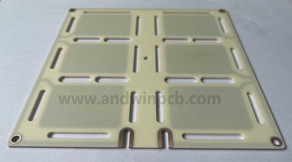
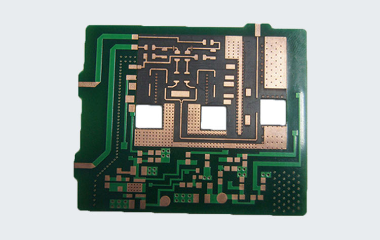
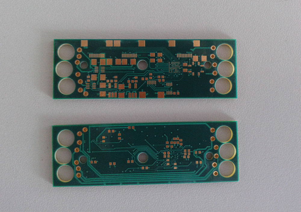
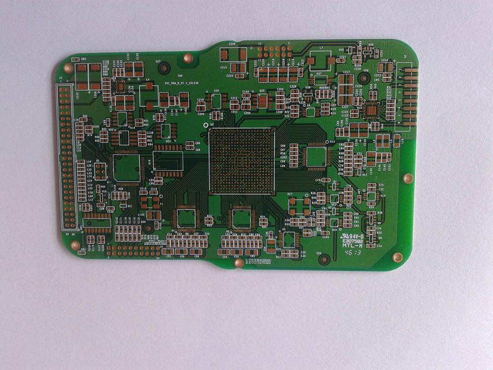
The pcbs provided by our company include Heavy copper PCB、Copper core PCB、Metal core PCB、High speed PCB、
Radio frequency PCB、HDI PCB