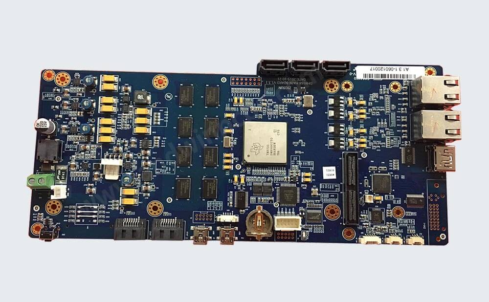
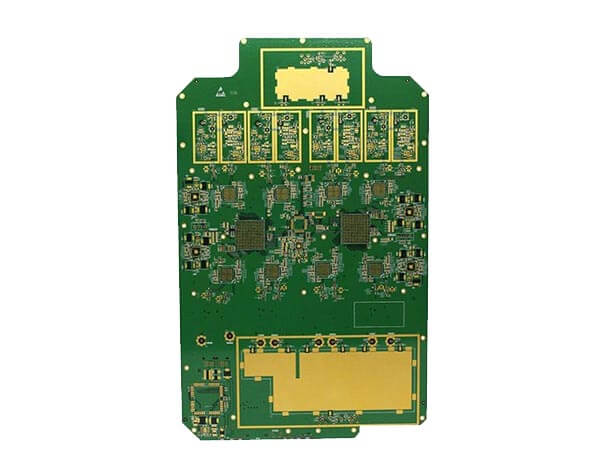
4 layers HDI PCB
4 Layers HDI PCBs are widely used in:
Telecom modules
wireless modules
LED display modules
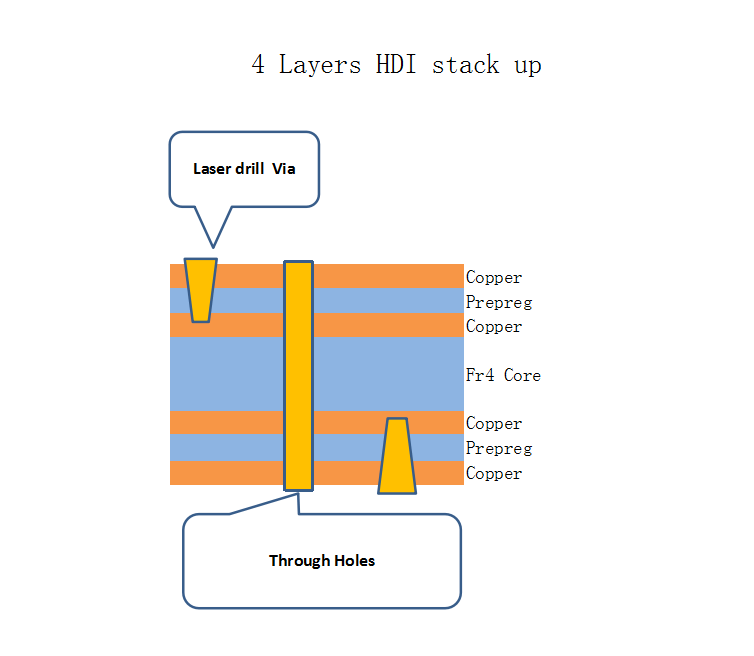
4 layers HDI PCB stack up
Technology
2 layer metal core pcb 4 layer pcb 4 layer pcb design 5G communication 6layer board stackup 7 layer board 8 layer board stackup 10 layer pcb 10 layer pcb stackup 12 layer pcb 12 layer pcb stackup 6035htc AD Series™ Antenna Materials aluminum clad pcb aluminum core pcb aluminum core pcb led aluminum pcb aluminum substrate PCB assemble electronic part assemble pcb
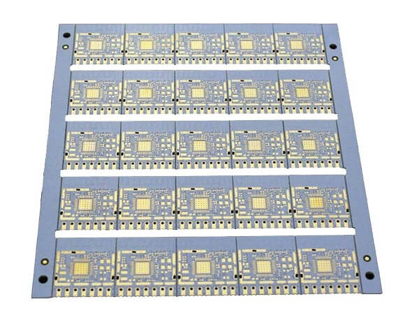
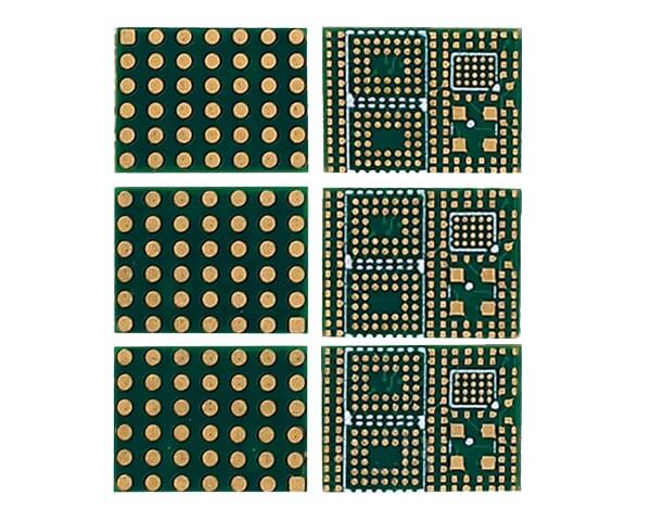
4 Layers HDI PCB samples
4 Layers HDI PCB
1.0mm TG 170
4 Layers HDI PCB
with Gold finger for connector
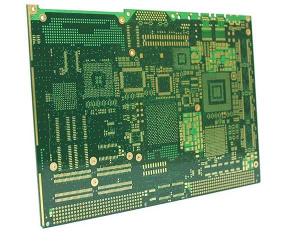
12 Layers High speed PCB prototype
Raw material: TU-872 SLK SP
10 Layers HDI PCB prototype
3 steps , 3+4+3
6 Layers HDI PCB prototype
For Blue tooth modules
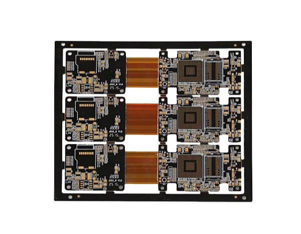
6 Layers Rigid flex PCB prototype
4 Layers PCB prototype
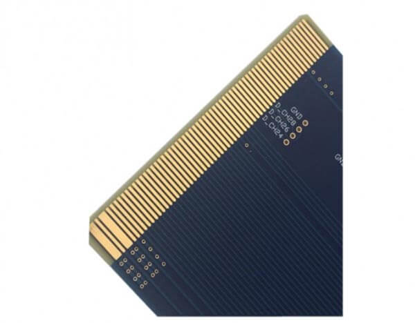
With Gold finger for connector
6 Layers HDI PCB prototype
2+2+2 for PCB module
4 Layers HDI PCB
Fastest lead time delivery in 3 days
Feature of HDI PCB
The HDI is an efficient and durable solution for creating high-functioning applications in a lighter and smaller format.
Along with all the improved functionality in smaller consumer products,
denser BGA, and QFP packages it lowers the heat transfer induced by stress.
The following features reflect the working process of HDI PCB in the applications:
The HDI PCB can get populated from both sides of the board and incorporate the components onto smaller boards.
It decreases the power consumption and leads to having longer stand-by facility into
The handheld and other battery-powered devices.
It comes in a well-built and rugged format to provide strength and limited perforations.
The reduced thermal degradation extends the endurance of the device.
The device can have higher density transmission and computational features using a smaller space.
The HDI PCB uses and accommodates with sustainable and dense BGA and QFP packages in
PCB technology design to create smaller devices based on the user’s demand.
It can be smartphones,aerospace equipment, medical applications, or military devices.
It enhances reliability in transmission whereas the PCB design gets into the point of mass production.
Benefits of HDI PCB
By the evolution of high-density PCB technology,
the engineers are having enough freedom and flexibility in designing the applications according to consumer demands.
They get space to place the components on both sides of the raw PCB. It consists of the following key benefits:
Concentrated Transfer of Heat:
The transfer of heat is reduced due to the close placement of the components.
The thermal expansion in HDI PCB also endures less stress and extends endurance.
Conductivity Management:
The vias in HDI PCB can be filled with conductive or non-conductive materials.
It can facilitate the transmission among the components and can customize according to the board design.
Improved functionality:
By using HDI PCB the functionality is improved as the blind vias and via-in-pad enables the components to be placed closely.
It increases the signal strength whereas the transmission range and the delay for transmitting time become less.
Smaller Form Factors:
The HDI PCB is better for saving space and the number of layers can be reduced without compromising the efficiency,
and durability as well as the design of the application device.
Non-conventional HDI Boards:
The HDI boards contain thinner lines,
Tighter spacing, and tighter annular ring using the thinner specialty materials.
For successful production of these boards right amount of time, investment, and manufacturing process.
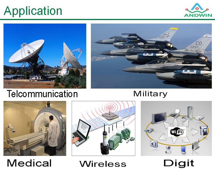
Applications of HDI PCB
HDI PCB is a complete solution to be used in a wide range of industries.
The efficiency is the key to these industries into certain types of applications and HDI PCB is perfect for that.
The following applications can be beneficial to use HDI PCB into the system:
Medical:
The medical industries require high definition application devices and HDI PCB has a great impact on that.
Medical devices work with the small package with high transmission rates.
HDI PCB fits into all sorts of medical devices that are used for implants,
labs, or imaging equipment making these devices more space-saving and cost-effective.
The HDI PCB can be used in small size cameras to observe the inner parts of the patients.
It makes sure the picture quality remains the same and accommodates the advancements.
Even some implants have to be small enough to fit inside of the human body,
with high signaling transmission rate and HDI PCB is just appropriate.
This also can be used in other medical equipment like emergency room monitors, CT scans, etc.
Military:
The military and defense applications require having highly efficient and durable PCB.
When certain devices are paired with high-density interconnected PCB,
That can even make it smaller in size can be a plus.
The HDI PCB can be incorporated in military applications especially into the
Communication devices and other strategic equipment such as missile and defense items.
Aerospace:
The applications used in aerospace work in an extremely rugged environment and need to ensure endurance for long term usage.
The HDI PCB can work properly under hazardous conditions which is ideal for aerospace applications.
Automotive:
The automobile manufacturing industries work with certain types of applications that have a high demand for smaller PCBs.
It can be a great help to save more space within the car.
With HDI PCB the cars can be programmed with some other exciting features like onboard GPS,
Wi-Fi, backup sensors, rearview mirrors, and so on.
Up to 10 layers of HDI are available with high demand in the market that can even introduce with futuristic cars.
Such integration of electronic devices offers a better driving experience which is the key focus to the carmakers.
Other main applications of HDI PCB
Electronic Devices:
HDI PCB has made it possible to create innovative gadgets from huge computers to laptops.
It is appropriate for multiple electronic devices like smartphones and tablets along with the
wearable devices VR headsets or Bluetooth headphones.
The prime idea for these applications is miniaturization and the highest level of efficiency.
For smartphones,
Every Layer Interconnection/ELIC type HDI PCB is required to make the devices thinner, smaller, and more portable.
Now it is also used in refrigerators, smart TVs, thermostats, etc.
The modern devices have the tendency to become thinner and smaller and PCBs are the major requirement.
The HDI PCBs come with benefits to amplify the functionality of circuit boards.
The development in the board technology makes it space-saving assisting the superiority of gadgets and other application devices.
The interconnected HDI PCB has been launched with the ability to
provide the ultimate results to the faster signal transmission with enhanced signaling quality.
It enhances the electrical performance of the device such as mobile phones,
Touch screen devices, laptop computers, digital cameras, 4G network communications as well as
The prominently featured applications used in medical, aircraft, military, and so on.
Get professional one stop PCB solution from us!
Other PCB products, you may interesting