
7 must-know tips for PCB design
1. What is the relationship between the line width and via hole size on the PCB board and the current flowing through it?
The thickness of the copper foil of a general PCB is 1 ounce, which is about 1.4 mil. The maximum current allowed for a line width of 1 mil is approximately 1 A. Via holes are relatively complex. In addition to the size of the via pad, it is also related to the thickness of the copper deposited on the hole wall after electroplating during the processing.
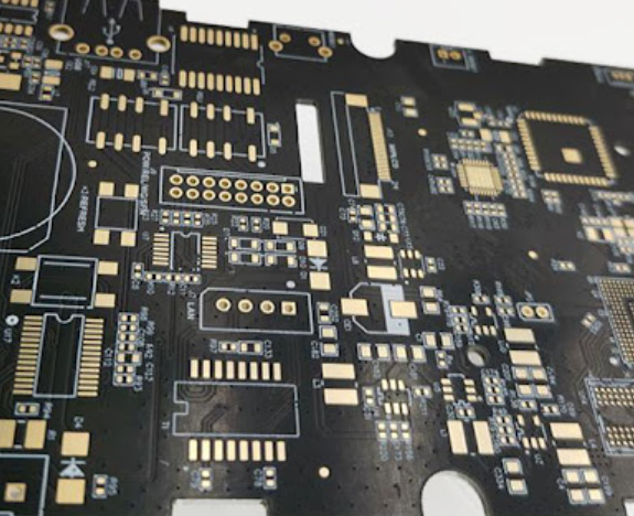
2. Why do you need to convert PCB files into GERBER files and drilling data before submitting them to the PCB factory for board manufacturing?
Most engineers are used to designing the PCB files and sending them directly to the PCB factory for processing. However, the more popular practice in the world is to convert the PCB files into GERBER files and drilling data and then submit them to the PCB factory. Why do this?
Because electronic engineers and PCB engineers have different understandings of PCB, the GERBER file converted by the PCB factory may not be what you want. For example, if you define the parameters of the components in the PCB file during design, you do not want these parameters to be displayed. On the finished PCB, you did not explain it. The PCB factory followed the example and left these parameters on the finished PCB.
This is just an example. If you convert PCB files to GERBER files yourself, you can avoid such incidents.
The GERBER file is an international standard light painting format file. It contains two formats: RS-274-D and RS-274-X. RS-274-D is called the basic GERBER format and must be accompanied by a D code file. Completely describes a graphic; RS-274-X is called the extended GERBER format, which itself contains D code information. Commonly used CAD software can generate files in these two formats.
How to check the correctness of the generated GERBER? You only need to import these GERBER files and D code files in the free software Viewmate V6.3 to see them on the screen or print them out through a printer.
Drilling data can also be generated by various CAD software. The general format is Excellon and can also be displayed in Viewmate. Of course, PCB cannot be made without drilling data.

3. How to improve the pass rate?
Completing the design of a printed circuit board generally requires processes such as schematic input – network table generation – Keepout Layer definition – network table (component) loading – component layout – automatic (manual) wiring.
Several popular software on the market today are not very powerful in the automatic component layout function. Manual layout can often improve the layout rate, but please don’t forget to make full use of the Move to Gird function, which can automatically move components. To the grid intersection, it is of great benefit to improve the pass rate.
4. How to add Chinese characters to PCB files?
There are many ways to add Chinese characters to PCB files. My favorite method is the one that will be introduced below:
A. Prerequisite: Protel99 software should be installed in your PC and run normally.
B. Steps: Copy the client99.rcs English menu file in the windows directory to another directory and save it; download Protel99cn.zip, unpack it and copy the client99.rcs to the windows directory; then copy other files to Design In the Explorer 99 directory; after restarting the computer and running Protel99, the Chinese menu will appear. The function of adding Chinese characters can be realized in the Place|Chinese Characters menu.
5. If there are only four pieces of DDRmemory attached to the motherboard and the clock is required to reach 150Mhz, what are the specific wiring requirements?
150Mhz clock wiring requires minimizing the length of the transmission line and reducing the impact of the transmission line on the signal. If it still cannot meet the requirements, simulate it to see if matching, topology, impedance control and other strategies are effective.
6. After automatic copper floating, the floating copper will fill the blank space according to the position and wiring layout of the devices on the board.
But this will form a lot of sharp corners and burrs less than or equal to 90 degrees, which will discharge during the high-voltage test and fail the high-voltage test. I don’t know if there is any other way besides removing these sharp corners and burrs through manual correction after automatic copper floating. There is no other good way.
The problem of sharp corner floating copper in automatic copper floating is indeed a very troublesome problem. In addition to the discharge problem you mentioned, there are also processing problems caused by the accumulation of acid droplets during processing.
As a supplier of PCB boards, we guarantee to provide customers with high-quality products and personalized customized services, including Heavy copper PCB, Copper core PCB, Metal core PCB, Ceramic PCB, etc. If you need it please contact