
Aerospace PCB Assembly Standards: The Ultimate Zero-Defect Guide for Manufacturers
In low-earth orbit or at 35,000 feet, there are no repair technicians. A $100 million satellite deployment or a critical flight control system can catastrophically fail because of a single $2 counterfeit capacitor or a micro-fracture in a solder joint. For aerospace electronics engineers, procurement managers, and QA directors, “good enough” is a recipe for disaster.
Navigating the complex landscape of aerospace PCB assembly requires more than just skimming through standard guidelines. It demands a flawless execution of zero-defect manufacturing, stringent traceability, and advanced thermal management. In this deep-dive guide, we will decode the critical aerospace standards (AS9100D and IPC-A-610 Class 3), reveal battle-tested strategies to mitigate counterfeit components, explain the science of outgassing in vacuum environments, and provide actionable blueprints to secure your aerospace supply chain.
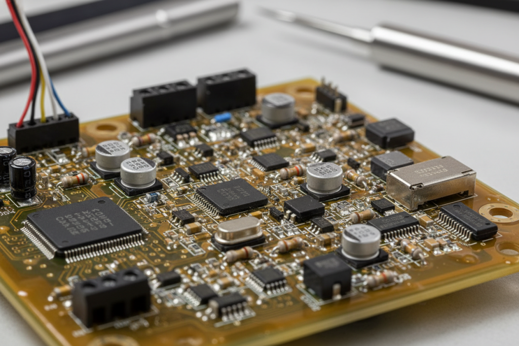
Understanding Aerospace PCB Standards: Why “Good Enough” is Never Enough
The aerospace and defense (A&D) sector operates under a unique set of physical and operational constraints. Unlike consumer electronics, aerospace printed circuit board assemblies (PCBAs) are subjected to extreme G-forces, aggressive vibrational profiles, massive thermal cycling (from -150°C in space shadows to +150°C in direct solar radiation), and the unforgiving vacuum of space.
For overseas B2B buyers and QA executives in North America and Europe, the primary pain points revolve around Zero-Tolerance for Failure and Supply Chain Integrity. You are not just buying a circuit board; you are investing in risk mitigation. A failure in a commercial aviation communication board or a satellite navigation module doesn’t just result in an RMA (Return Merchandise Authorization)—it risks human lives and catastrophic financial losses.
Therefore, partnering with a manufacturer that strictly adheres to aerospace standards is non-negotiable. It proves that the facility has the engineering maturity to handle extreme environmental testing, rigorous vendor qualification, and exhaustive documentation for every single component placed on the board.
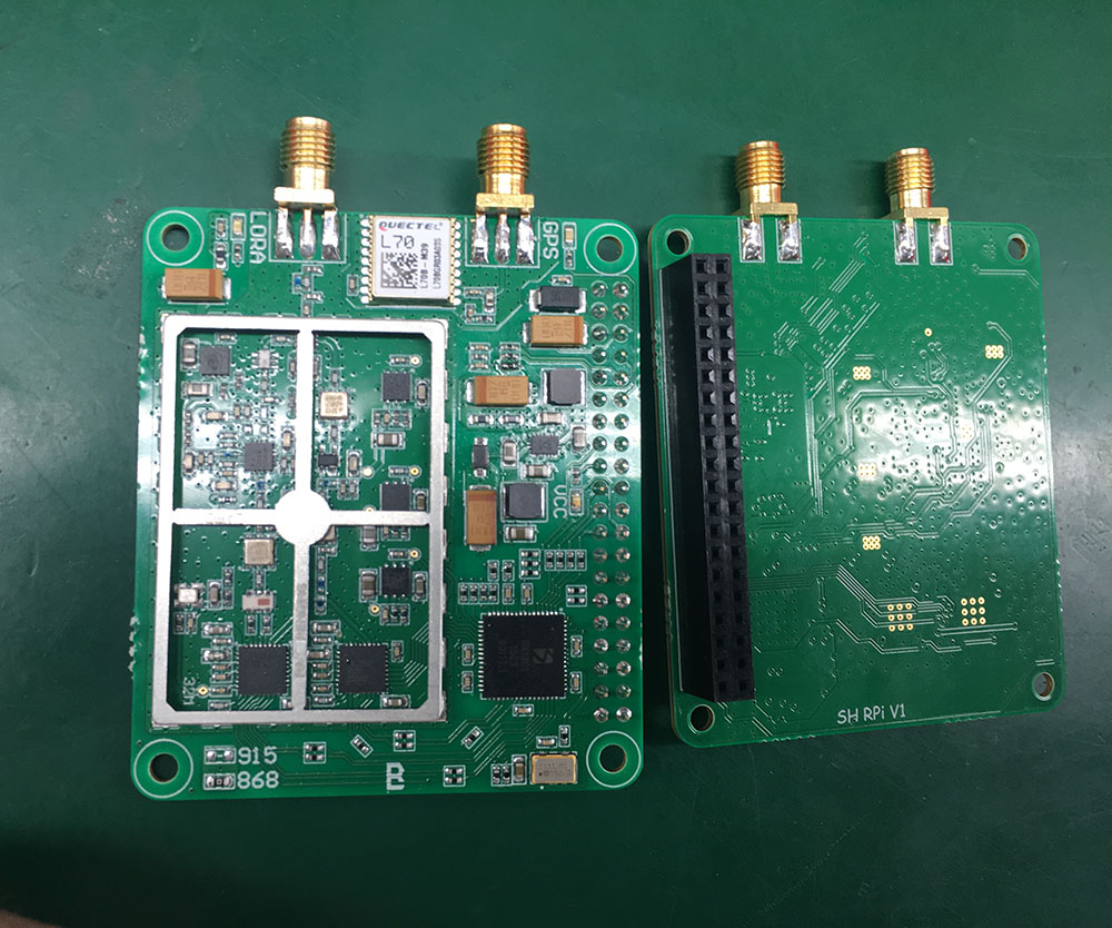
Core Concepts Simplified: AS9100D & IPC-A-610 Class 3
When vetting a manufacturer, you will constantly hear two terms: AS9100D and IPC-A-610 Class 3. Let’s translate these from dry regulatory jargon into plain English.
AS9100D: The “Birth Certificate” of Your PCBA
Think of AS9100D not as a manufacturing technique, but as an unbreakable chain of custody. It is a quality management system (QMS) specifically designed for aerospace. If ISO 9001 is a basic background check, AS9100D is a full-scale forensic investigation. It ensures that every single element—from the raw copper laminate to the microscopic resistors—has a traceable “birth certificate.” If a component fails in the field five years later, AS9100D ensures you can trace that exact component back to the specific reel, the specific operator who soldered it, and the exact date it was manufactured.
IPC-A-610 Class 3: The “No Downtime” Mandate
IPC-A-610 is the universally accepted standard for electronic assembly acceptance. While Class 1 is for cheap toys and Class 2 is for standard laptops, Class 3 is the highest tier. It mandates uninterrupted, continuous high performance in exceptionally harsh environments. In Class 3, there is zero tolerance for anomalies like solder voids, misalignments, or insufficient barrel fill in through-holes.
To understand how this compares to other industries, especially when evaluating automotive and industrial standards, refer to the comparison table below:
Comparison Table: PCB Assembly Classes & Standards
| Feature / Requirement | IPC Class 2 (Standard Industrial) | IPC Class 3 (Aerospace & Medical) | Why it Matters for Aerospace |
|---|---|---|---|
| Operational Mandate | Continuous operation is desired, but not critical. | Continuous performance or performance on demand is critical. | Equipment downtime cannot be tolerated in flight. |
| Through-Hole Solder Fill | Minimum 50% vertical fill. | Minimum 75% vertical fill (often pushed to 100%). | Ensures structural integrity during extreme vibration. |
| Component Placement | Slight overhang allowed. | Exacting precision, minimal to zero overhang. | Prevents mechanical stress fractures under G-forces. |
| Traceability | Lot-level traceability. | 100% component and operator-level traceability. | Crucial for identifying counterfeit or defective batches. |
| Quality Management | ISO 9001 | AS9100D | Embeds aerospace-specific risk and configuration management. |
The Zero-Defect Blueprint: Step-by-Step Guide to Aerospace PCBA
Achieving aerospace-grade reliability requires a systematic, almost paranoid approach to manufacturing. Here is the operational blueprint that top-tier manufacturers use to eliminate risks.
Scenario A: Counterfeit Component Mitigation & 100% Traceability
One of the most discussed nightmares on engineering forums like Reddit’s r/aerospace is the infiltration of counterfeit components from the gray market. Counterfeiters have become incredibly sophisticated, re-marking commercial-grade chips as aerospace-grade (military spec).
The Mitigation SOP (Standard Operating Procedure):
- Authorized Distributors Only: Procurement must be restricted to Original Component Manufacturers (OCMs) or franchised distributors.
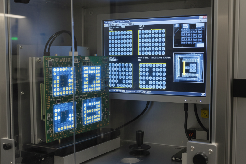
- X-Ray Inspection (AXI): Every incoming batch of high-value ICs must undergo 2D/3D X-ray inspection to verify the internal wire bonding and die size match the manufacturer’s original specifications.
- Decapsulation (De-capping): A destructive test where the plastic or ceramic packaging of a sample chip is chemically dissolved using fuming nitric acid. QA engineers then inspect the silicon die under a high-power microscope to verify the manufacturer’s logo and topography.
- XRF (X-ray Fluorescence) Testing: Used to verify the elemental composition of component leads, ensuring they meet strict RoHS or non-RoHS (leaded solder is still widely used in aerospace to prevent tin whiskers) requirements.
Scenario B: Material Selection to Survive Vacuum and Extreme Heat
Standard FR4 fiberglass boards are perfectly fine for your smart home devices, but send them into the vacuum of space, and you will encounter Outgassing.
The Outgassing Phenomenon:
In a high-vacuum environment, standard PCB laminates, plastics, and adhesives release trapped volatile organic compounds (VOCs) as gases. These gases can condense on sensitive optical lenses, star trackers, or satellite sensors, rendering them completely blind.
The Solution:
Aerospace engineers must select specialized materials. Polyimide is the gold standard. It offers exceptionally high thermal stability (high Tg – Glass Transition Temperature) and negligible outgassing. Manufacturers must test materials to ensure Total Mass Loss (TML) is < 1.0% and Collected Volatile Condensable Material (CVCM) is < 0.1%.
Furthermore, when dealing with advanced radar or communication systems, engineers must factor in high-speed routing considerations using low-loss materials like Rogers or Teflon (PTFE) to maintain signal integrity while surviving extreme temperatures.
Scenario C: Conformal Coating and Thermal Management
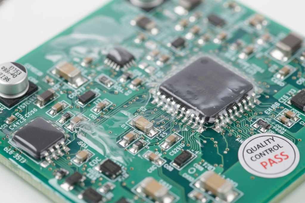
Think of Conformal Coating as a tailored spacesuit for your PCB. It is a micro-thin polymeric film applied over the assembled board to protect it from moisture, dust, chemicals, and extreme temperature variations.
For aerospace, standard acrylic coatings are insufficient. Parylene or Silicone conformal coatings are strictly required. Parylene is applied via chemical vapor deposition (CVD) in a vacuum chamber, ensuring a completely pinhole-free, uniform coating that penetrates even the smallest crevices beneath BGA components.
Thermal Management:
In space, there is no air to facilitate convective cooling. Heat generated by high-power processors must be conducted away through the board itself. This requires heavy copper planes (often 3 oz to 6 oz), thermal vias (micro-holes filled with conductive epoxy and plated over), and metal-core PCBs (MCPCB) to draw heat toward the chassis. Achieving this level of manufacturing requires adhering to strict precision requirements to ensure the thermal vias do not compromise the structural integrity of the board.
Expert Tips & Common Pitfalls to Avoid
Even with strict standards, manufacturers and engineers often fall into traps that cost time and money. Based on real-world experiences from industry veterans and QA audits, here are the most common pitfalls to avoid.
Pitfall 1: Insufficient Cleaning Before Conformal Coating
The Problem: Conformal coating delamination (peeling). Many manufacturers assume no-clean flux doesn’t need cleaning. In aerospace, “no-clean” is a myth. Any flux residue trapped under the coating will cause the coating to blister and peel during extreme temperature cycling.
The Fix: Implement a rigorous multi-stage aqueous wash and ionic contamination testing (ROSE testing) before applying any coating.
Pitfall 2: Ignoring CTE (Coefficient of Thermal Expansion) Mismatch
The Problem: When the PCB material and the ceramic components expand and contract at different rates during temperature swings, it shears the solder joints apart.
The Fix: Match the CTE of the PCB substrate closely to the critical components, or use compliant leads that can absorb the mechanical stress.
Pitfall 3: Tin Whiskers in Lead-Free Solder
The Problem: Pure tin (lead-free) finishes can grow microscopic conductive “whiskers” in space, causing catastrophic short circuits.
The Fix: Despite global RoHS regulations, the aerospace and military sectors often mandate the use of leaded solder (Sn63Pb37) to completely eliminate the risk of tin whiskers.
Specification / Data Table for Aerospace PCB Material Selection
When comparing options with your manufacturer, use this data table as your baseline for material specifications:
| Parameter | Standard Commercial (FR4) | Aerospace Grade (Polyimide / Rogers) | Aerospace Requirement |
|---|---|---|---|
| Tg (Glass Transition Temp) | 130°C – 140°C | 200°C – 250°C+ | Must withstand > 170°C without softening. |
| Td (Decomposition Temp) | ~300°C | > 350°C | Prevents structural breakdown during heavy soldering. |
| TML (Total Mass Loss) | > 2.0% (Fails vacuum test) | < 1.0% | Prevents Outgassing in space. |
| Moisture Absorption | 0.20% – 0.25% | < 0.10% | Prevents micro-cracking during rapid freezing. |
| Surface Finish | HASL (Lead-Free) | ENIG, ENEPIG, or HASL (Leaded) | Must prevent tin whiskers and ensure flat pads. |
Conclusion & Final Thoughts
Manufacturing aerospace electronics is not about finding the cheapest vendor; it is about finding a partner obsessed with risk mitigation. From understanding the rigorous documentation of AS9100D and the zero-defect mandate of IPC-A-610 Class 3, to implementing aggressive anti-counterfeiting measures and mastering vacuum-safe materials, every step must be executed with absolute precision.
Do not compromise on traceability, do not skip destructive testing for components, and ensure your manufacturer understands the physics of outgassing and thermal expansion.
Quick Summary Table: Aerospace PCBA Checklist
| Critical Area | Key Action Item | Goal |
|---|---|---|
| Compliance | Verify AS9100D and IPC Class 3 capabilities. | Ensure zero-defect manufacturing and full traceability. |
| Supply Chain | Mandate X-ray, Decapsulation, and Authorized Distributors. | Block counterfeit components from entering the build. |
| Materials | Specify Polyimide/PTFE with TML < 1.0%. | Prevent outgassing and survive extreme thermal cycling. |
| Protection | Demand Parylene coating and ionic contamination testing. | Protect against moisture, vacuum, and chemical exposure. |
If you are navigating the complexities of high-reliability manufacturing and need a partner who understands the uncompromising nature of aerospace standards, it is time to upgrade your supply chain. Explore reliable PCB assembly services that combine state-of-the-art inspection technology with strict AS9100D compliance to ensure your next mission is a resounding success.
Frequently Asked Questions (FAQ)
Q1: What is the difference between IPC Class 2 and IPC Class 3 for aerospace PCBs?
IPC Class 2 allows 50% through-hole solder fill and slight component overhang—acceptable for standard industrial equipment. IPC Class 3 mandates 75%+ solder fill, exacting placement precision, and zero tolerance for anomalies. In aerospace, Class 3 is non-negotiable because equipment downtime during flight is catastrophic.
Q2: Why does aerospace still use leaded solder despite RoHS regulations?
Pure tin (lead-free) finishes grow microscopic conductive “whiskers” over time, especially in the vacuum and thermal cycling of space. These whiskers can bridge traces and cause short circuits. Leaded solder (Sn63Pb37) completely eliminates this risk, which is why aerospace and military sectors often mandate it despite environmental regulations.
Q3: What is outgassing and why does it matter for space applications?
Outgassing is the release of trapped volatile organic compounds (VOCs) from PCB materials in high-vacuum environments. These gases condense on optical lenses, star trackers, and sensors, rendering them blind. Aerospace-grade materials like Polyimide must pass NASA standards: Total Mass Loss (TML) < 1.0% and Collected Volatile Condensable Material (CVCM) < 0.1%.
Q4: How do manufacturers prevent counterfeit components in aerospace supply chains?
Top-tier manufacturers implement a three-layer defense: (1) procurement restricted to authorized OCMs and franchised distributors only; (2) 100% batch X-ray inspection (AXI) to verify internal die geometry; (3) destructive decapsulation sampling using fuming nitric acid to inspect silicon topography under high-power microscopy. SAE AS5553 compliance is mandatory.
Q5: Why is Parylene preferred over standard acrylic conformal coating for aerospace?
Standard acrylic coatings are applied by spraying or brushing, leaving pinholes and uneven thickness. Parylene is deposited via Chemical Vapor Deposition (CVD) in a vacuum chamber, creating a completely pinhole-free, uniform film that penetrates beneath BGA components. It provides superior moisture and chemical protection without adding significant weight—critical for space missions.