
The Ultimate Guide to Silicon Carbide PCB Substrates for High-Temperature Electronics
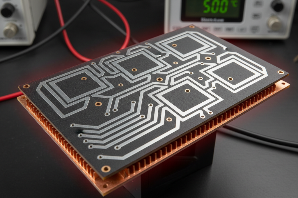
If you are designing high-power electronics, EV motor drives, or aerospace power modules, you already know the harsh truth: traditional FR4 chars and delaminates at 130°C. Even standard Alumina (Al2O3) ceramic substrates begin to show micro-cracks under the extreme thermal cycling of modern Wide Bandgap (WBG) semiconductors. When your junction temperatures routinely exceed 200°C, and failure is not an option, standard materials become the bottleneck of your entire system.In this comprehensive guide, we will break down the engineering realities of Silicon Carbide (SiC) PCB substrates. You will learn exactly why SiC is dominating high-temperature electronics, how to justify its ROI against cheaper alternatives, and how to navigate the notorious manufacturing challenges that plague junior designers.
If you are exploring the broader landscape of thermal management before committing to a specific material, we highly recommend reviewing our comprehensive guide on advanced ceramic PCB solutions to understand the baseline capabilities of ceramic technology.
Understanding Silicon Carbide (SiC) PCB Substrates: The Basics
The electronics industry is undergoing a massive shift driven by the electrification of vehicles (EVs), renewable energy inverters, and high-density power grids. At the heart of this revolution are Wide Bandgap (WBG) semiconductors—specifically SiC and GaN bare dies. These chips can handle exponentially higher voltages and switch at blistering speeds, but they generate intense, localized heat fluxes that traditional packaging simply cannot survive.
Why the Shift to SiC Substrates?
For decades, engineers relied on Direct Bond Copper (DBC) Alumina for power modules. However, as power density increases, the limitations of Alumina become painfully obvious: its thermal conductivity (around 24-28 W/m·K) acts as a thermal bottleneck. Heat gets trapped beneath the die, forcing designers to employ aggressive thermal derating—artificially limiting the performance of an expensive SiC chip just to keep it from melting its own solder joints.
Silicon Carbide (SiC) PCB substrates eliminate this bottleneck. By utilizing SiC as the foundational insulating layer, engineers achieve a thermal conductivity that rivals premium metals, combined with the electrical isolation of a high-grade ceramic. This allows power electronics designers to push their WBG devices to their absolute maximum ratings, shrinking the overall size of the cooling apparatus (heatsinks, liquid cooling plates) and significantly reducing the overall system weight—a critical metric in automotive and aerospace applications.
Core Concepts Simplified
To truly grasp why SiC substrates command a premium price, we must translate complex material science into practical engineering benefits. Here is how SiC solves the three biggest headaches in high-temperature electronics.
Superior Thermal Management (The “Sports Car Radiator” Analogy)
Imagine you just dropped a 1,000-horsepower V8 engine (your new SiC MOSFET) into a compact car. If you use the factory-standard radiator (FR4 or Alumina), the engine will overheat in minutes, forcing you to drive at 30 mph to prevent a blowout.
A SiC substrate is the equivalent of a custom-built, liquid-cooled, super-car radiator. With a thermal conductivity ranging from 120 to 170 W/m·K, it pulls heat away from the die dozens of times faster than standard materials. This rapid heat dissipation means you can say goodbye to thermal derating. Your components run cooler, switch faster, and last longer, even when operating continuously in ambient temperatures exceeding 200°C.
High-Temperature Reliability & CTE Matching (The “Shoe and Foot” Analogy)
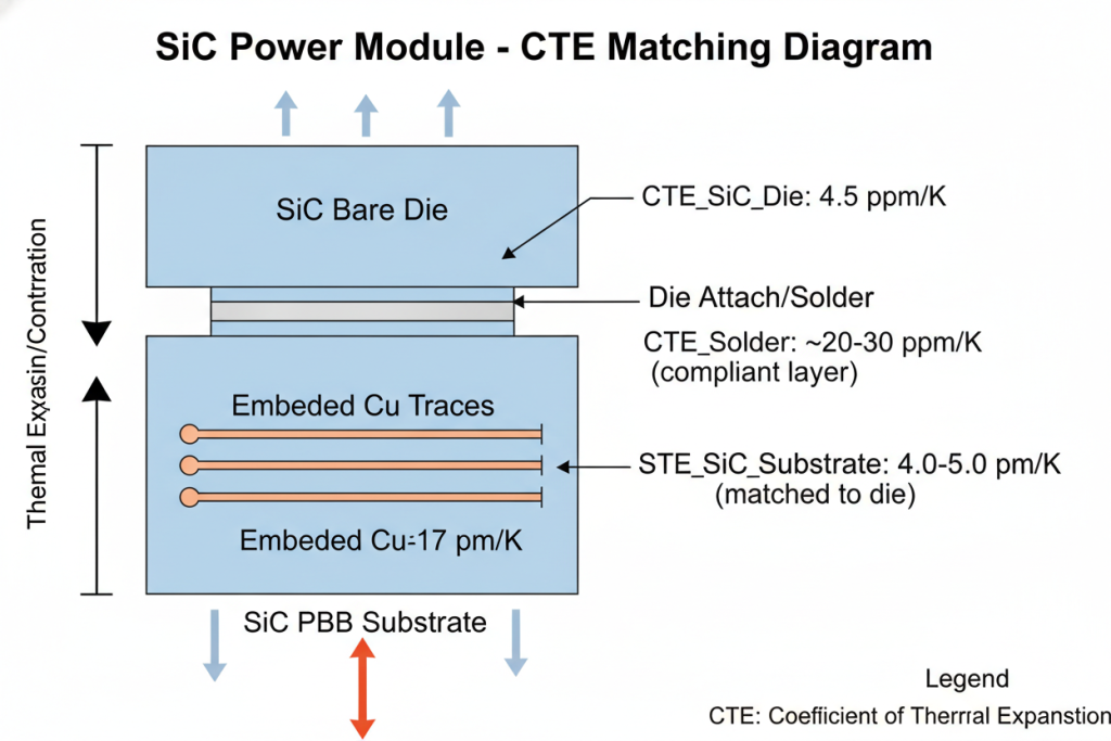
Coefficient of Thermal Expansion (CTE) measures how much a material swells when heated. Think of the PCB substrate as a shoe, and the silicon or SiC bare die as your foot.
If you go for a run and your foot swells, but your rigid leather shoe does not, you get blisters. In electronics, if the copper trace expands rapidly (CTE ~17 ppm/°C) but the ceramic underneath expands slowly, the resulting thermo-mechanical stress literally tears the solder joints apart or cracks the ceramic.
SiC substrates have a CTE of approximately 4.0 ppm/°C. This is essentially a perfect match for SiC bare dies. When the system heats up from 25°C to 250°C, the die and the substrate expand at the exact same rate. The “shoe” fits perfectly, eliminating the shear stress that causes fatigue failures in high-power thermal cycling.
Wide Bandgap (WBG) & Dielectric Strength
Dielectric Strength is the maximum voltage a material can withstand before it fails and allows current to arc through it. Because SiC is a Wide Bandgap material, it requires significantly more energy to knock its electrons loose. This means a relatively thin layer of SiC ceramic can block massive amounts of voltage (often rated in tens of thousands of volts per millimeter). You can design a thinner substrate, which further reduces the thermal resistance path from the chip to the heatsink.
Core Concept Comparison Table
To put SiC into perspective, here is how it stacks up against standard power electronics substrates:
| Material Property | FR4 (Standard PCB) | Alumina (Al2O3) | Aluminum Nitride (AlN) | Silicon Carbide (SiC) |
|---|---|---|---|---|
| Thermal Conductivity (W/m·K) | 0.3 – 0.4 | 24 – 28 | 170 – 230 | 120 – 170 |
| CTE (ppm/°C) | 14 – 17 | 7.0 – 8.0 | 4.5 | ~4.0 (Perfect for SiC dies) |
| Dielectric Strength (kV/mm) | ~20 | ~15 | ~15 | >20 |
| Mechanical Toughness | High | Low (Brittle) | Moderate | High |
| Cost Profile | Very Low | Low | High | Premium |
Material Selection & Application Scenarios
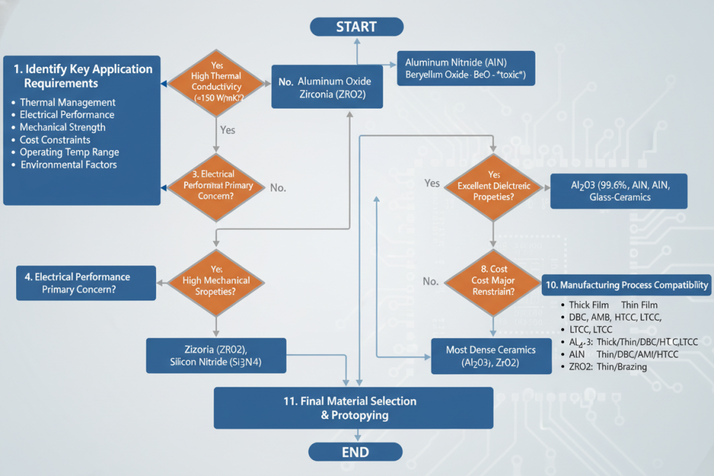
Choosing a SiC substrate is not a universal solution; it is a calculated engineering decision based on ROI. Because processing SiC is notoriously difficult (it is nearly as hard as diamond), the substrates carry a premium price tag. Here is a step-by-step decision framework to help you justify the cost.
Scenario A: EV Powertrains & High-Voltage Traction Inverters
The Challenge: Electric vehicle traction inverters must convert massive amounts of DC power from the battery into AC power for the motor. They operate in harsh, under-hood environments where ambient temperatures are high, and liquid cooling systems add unwanted weight.
The Solution: By pairing SiC MOSFETs with a SiC PCB substrate via Active Metal Brazing (AMB), designers can achieve unparalleled power density.
- Actionable Step: When designing for >800V EV architectures, specify AMB SiC substrates. The AMB process chemically bonds thick copper (up to 0.8mm) to the SiC ceramic, providing immense current-carrying capacity while surviving thousands of extreme temperature shock cycles (-40°C to +250°C) without delamination.
Scenario B: Balancing Budget, Thermal, and Mechanical Constraints
If SiC is overkill for your budget, or if you have specific mechanical requirements, you must pivot to alternative ceramics. Use this decision matrix:
- Need extreme thermal conductivity but lower cost than SiC?
If you are using standard Silicon IGBTs rather than SiC dies, Aluminum Nitride (AlN) offers incredible thermal performance. However, AlN is relatively brittle. To understand the cost-to-performance ratio, review our detailed breakdown on Silicon Nitride vs Alumina PCB to see where your budget fits. - Need extreme mechanical toughness for high-vibration environments?
If your PCB will be mounted in aerospace turbines or heavy industrial drilling equipment, thermal conductivity might take a back seat to fracture toughness. In these cases, Zirconia ceramic PCB is the superior choice due to its “self-healing” phase transformation properties that stop crack propagation. - Need ultra-high thermal performance for RF/Microwave applications?
If you are dealing with high-frequency RF where dielectric constant matters as much as heat, you might explore exotic materials. Read our Beryllium Oxide (BeO) vs Boron Nitride (BN) guide. Note: BeO requires strict safety handling due to toxicity, making SiC or AlN safer alternatives for general power electronics.
Specification Data Sheet for High-Power Scenarios
Use this template when drafting your procurement specifications or communicating with your PCB manufacturer:
| Parameter | Recommended Spec for 800V+ EV Inverters | Reasoning |
|---|---|---|
| Substrate Material | Silicon Carbide (SiC) or Silicon Nitride (Si3N4) | Optimal CTE match and thermal conductivity. |
| Metallization Process | Active Metal Brazing (AMB) | DBC (Direct Bond Copper) fails under extreme thermal cycling. AMB provides superior peel strength. |
| Copper Thickness | 0.3mm to 0.8mm | Required for high current carrying capacity (hundreds of Amps). |
| Surface Finish | ENEPIG or ENIG | Prevents copper oxidation at 200°C+ and provides a perfectly flat surface for die attach. |
| Die Attach Method | Silver Sintering | Standard solder melts at high temps. Sintered silver provides a high-temp, highly conductive bond. |
Expert Tips & Common Pitfalls to Avoid
When browsing hardware engineering forums like Reddit’s r/PrintedCircuitBoard or the EEVblog forums, you will frequently see engineers complaining about expensive ceramic PCB failures. Here is the unvarnished truth about working with SiC substrates and how to avoid costly prototyping mistakes.
🔴 Pitfall 1: Assuming Direct Bond Copper (DBC) works for everything
The Mistake: Junior engineers often specify DBC for SiC substrates to save money.
The Reality: DBC relies on a high-temperature oxidation process to bond copper to the ceramic. While this works decently for Alumina, SiC and AlN do not form strong oxide layers easily. Under severe thermal cycling, DBC traces on SiC will peel off like cheap tape.
The Fix: Always specify Active Metal Brazing (AMB) for SiC and AlN substrates. AMB uses a brazing alloy (often containing titanium) that chemically reacts with the ceramic, creating a bond so strong that the ceramic itself will fracture before the copper peels.
🔴 Pitfall 2: Ignoring Machining Costs and Tolerances
The Mistake: Designing intricate cutouts, complex outlines, or hundreds of microvias in a SiC substrate as if it were FR4.
The Reality: Silicon Carbide has a Mohs hardness of 9 to 9.5 (Diamond is 10). You cannot route it with standard CNC bits; they will be destroyed instantly. SiC must be laser-cut or machined using expensive diamond tooling.
The Fix: Keep your PCB outline as simple as possible (rectangles or squares). Minimize the number of holes. If vias are absolutely necessary, consult with your manufacturer early about laser-drilling capabilities and aspect ratios.
🔴 Pitfall 3: Over-specifying for Low-Power Applications
The Mistake: Using a SiC substrate for a standard 12V automotive LED driver just because it runs “a bit hot.”
The Reality: You will blow your budget instantly. SiC is a premium material designed for hundreds of volts and extreme power densities.
The Fix: If your junction temperature is below 150°C and you are not using SiC bare dies, stick to standard Metal Core PCBs (MCPCB) or Alumina. Reserve SiC for applications where the ROI of eliminating heavy heatsinks justifies the substrate cost.
Conclusion & Final Thoughts
Transitioning to Silicon Carbide (SiC) PCB substrates is not just a material upgrade; it is a fundamental shift in how power electronics are architected. By leveraging its extraordinary thermal conductivity (up to 170 W/m·K) and perfect CTE matching for SiC bare dies, engineers can unlock the true potential of Wide Bandgap semiconductors.
Yes, the material is expensive. Yes, it requires specialized AMB metallization and laser machining. But in industries like EV manufacturing, aerospace, and renewable energy, the ability to eliminate massive liquid cooling systems, prevent thermal derating, and ensure decades of reliability makes SiC an investment that pays for itself many times over.
Quick Summary
| Feature | The Engineering Benefit | Bottom Line Impact |
|---|---|---|
| Extreme Thermal Conductivity | Rapid heat dissipation from high-power dies. | Eliminates thermal derating; allows for smaller heatsinks. |
| Matched CTE (~4.0 ppm/°C) | Expands at the same rate as SiC chips. | Prevents solder joint fatigue and mechanical failure. |
| High Dielectric Strength | Withstands massive voltage in a thinner profile. | Enables compact, high-voltage power modules. |
| AMB Compatibility | Forms unbreakable bonds with thick copper. | Allows handling of hundreds of Amps safely. |
Ready to optimize your high-temperature power modules?
Before finalizing your Gerber files, ensure your manufacturer has the specialized equipment required for AMB processing and diamond-tool machining. If you are still weighing your options, explore our extensive resources on ceramic materials to find the perfect balance of performance and budget for your next breakthrough design.
Frequently Asked Questions (FAQ)
Q1: Why choose SiC over standard Alumina for high-power electronics?
Alumina (24–28 W/m·K) creates a severe thermal bottleneck under modern power densities. SiC substrates deliver 120–170 W/m·K, pulling heat away from the die up to 6x faster. This eliminates thermal derating, lets you run WBG semiconductors at full spec, and shrinks your cooling system.
Q2: What is AMB and why is it mandatory for SiC substrates?
Active Metal Brazing (AMB) uses a titanium-based alloy to chemically bond copper to SiC. Standard Direct Bond Copper (DBC) relies on oxide layers that SiC cannot form reliably. Under thermal cycling, DBC traces peel off. AMB creates a bond so strong the ceramic fractures before the copper delaminates.
Q3: Can I use standard PCB machining tools on SiC?
No. SiC has a Mohs hardness of 9–9.5 (diamond is 10). Standard CNC bits are destroyed instantly. SiC requires laser cutting or diamond tooling. Keep your design simple—rectangular outlines, minimal holes—to control machining costs.
Q4: When is SiC overkill and what should I use instead?
If your junction temperature stays below 150°C and you are not using SiC bare dies, SiC is economically unjustified. For standard applications, use Metal Core PCB (MCPCB) or Alumina. Reserve SiC for >800V EV inverters, aerospace power modules, or any system where eliminating heavy heatsinks justifies the premium.
Q5: How does CTE matching prevent solder joint failure?
CTE measures how much a material expands when heated. SiC substrates have a CTE of ~4.0 ppm/°C, nearly identical to SiC bare dies. When the system cycles from -40°C to +250°C, die and substrate expand in unison. Mismatched CTE (e.g., copper at 17 ppm/°C on Alumina at 7–8 ppm/°C) creates shear stress that cracks solder joints and delaminates traces over time.