
PCB Testing Methods: AOI, X-Ray, Flying Probe, and ICT Explained
A finished board can pass one test and fail the next, because each method looks for a different kind of defect. AOI sees a missing part in seconds but is blind to the solder ball hidden under a BGA. ICT measures a resistor’s value but never proves the board boots. Choose the wrong method and defects ship; stack too many and your test cost eats the margin.
The real decision is not “do we test,” but which methods, in what order, and at what volume the cost is justified. This guide breaks down the four core methods, what each one actually catches, and how to sequence them.
Inspection vs Electrical Test
The four methods split into two families. Inspection (AOI and X-ray) checks that parts are present, aligned, and soldered correctly. It sees geometry, not function. Electrical test (flying probe and ICT) applies signals and measures the response, so it catches a wrong-value resistor or an open that looks perfect under a camera.
Neither family replaces the other. A joint can look flawless and be electrically open; a net can pass continuity while a tombstoned cap sits crooked. Good PCB assembly uses both.
Automated Optical Inspection (AOI)
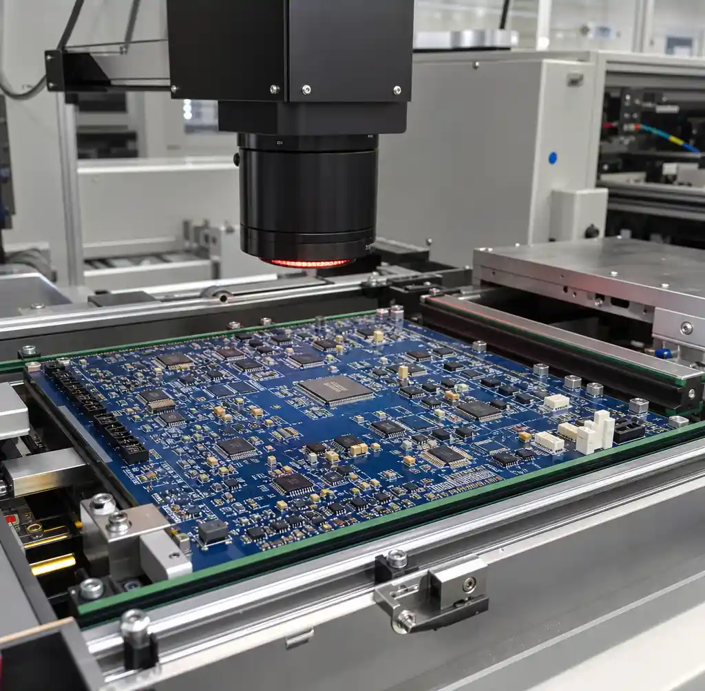
AOI uses high-resolution cameras and lighting to compare each board against a known-good reference. It runs inline in 10–20 seconds per board and flags missing components, wrong parts, tombstoning, bridges, misalignment, and polarity errors. It is your first line of defense right after reflow.
The upgrade that matters is 3D AOI. Instead of flat 2D images, it projects structured light to measure solder-joint height and volume, which catches insufficient paste and lifted leads that 2D misses. Pair it with solder paste inspection (SPI) before reflow and you catch paste defects before a single part is placed.
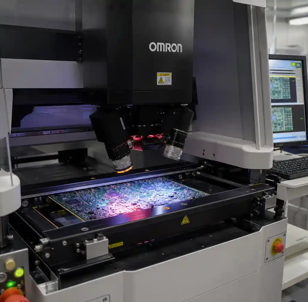
The newest gain is AI. Deep-learning classifiers now cut false calls sharply versus rule-based systems, so operators spend less time clearing good boards flagged as bad. Published work reports inspection accuracy above 99% on trained defect sets. AOI’s hard limit stays the same, though: it only sees what light can reach. Any joint hidden under a package body is invisible to it.
X-Ray Inspection (AXI)
X-ray inspection sees through the package to the joint underneath. That makes it the only practical way to inspect BGAs, QFNs, and bottom-terminated components whose solder balls sit where no camera can look. It images opens, shorts, insufficient solder, and voiding inside a joint.
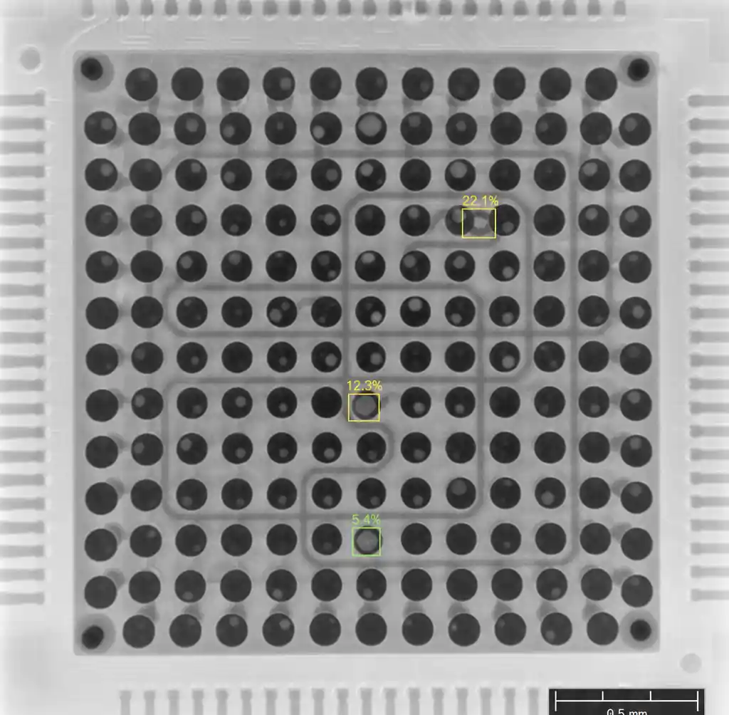
Voiding is where X-ray earns its keep. Trapped gas inside a solder ball weakens the joint and hurts thermal transfer. IPC-A-610 sets the common acceptance limit at 25% voiding by area for a BGA ball; X-ray is how you measure it. 2D X-ray suits most single-sided cases, while 3D CT (computed tomography) slices double-sided and stacked assemblies where joints overlap.
X-ray is slower and more expensive per board than AOI, so it is applied to the risk areas, not every joint. On dense boards used in HDI designs and medical or automotive work, that targeted coverage is non-negotiable.
Flying Probe Test
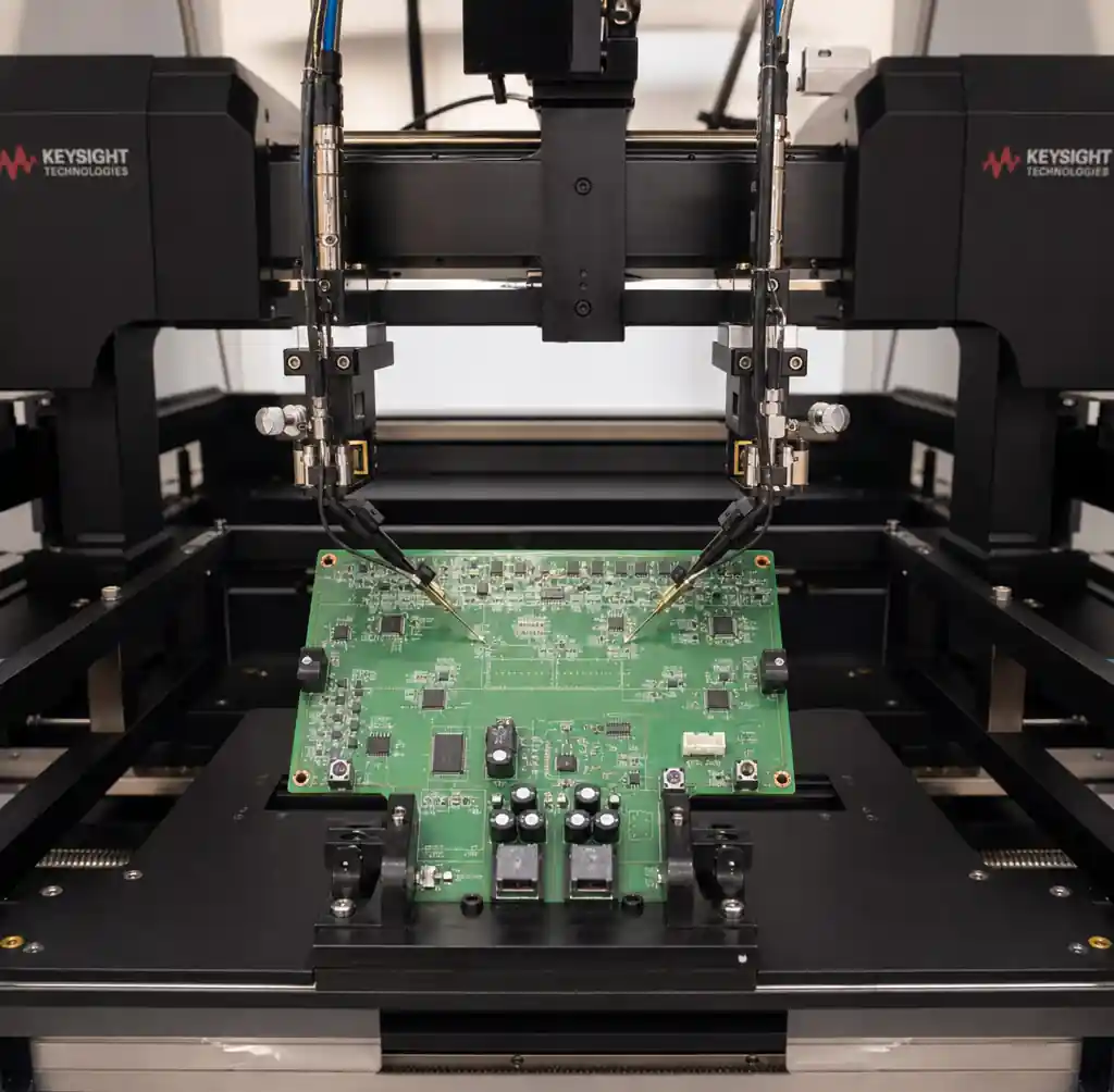
Flying probe is electrical test without a fixture. Two to eight motorized probes move across the board, touching test pads and pins to measure resistance, capacitance, opens, and shorts, guided by the netlist. Because there is no tooling to build, it starts testing within hours of receiving the design.
That flexibility is why it owns prototypes, quick-turn assembly, and low-volume runs. When a board revision changes the netlist, you reload the program instead of scrapping a fixture. The trade-off is speed: probing every net sequentially takes roughly 3–8 minutes per board, so it does not scale to thousands of units.
In-Circuit Test (ICT)
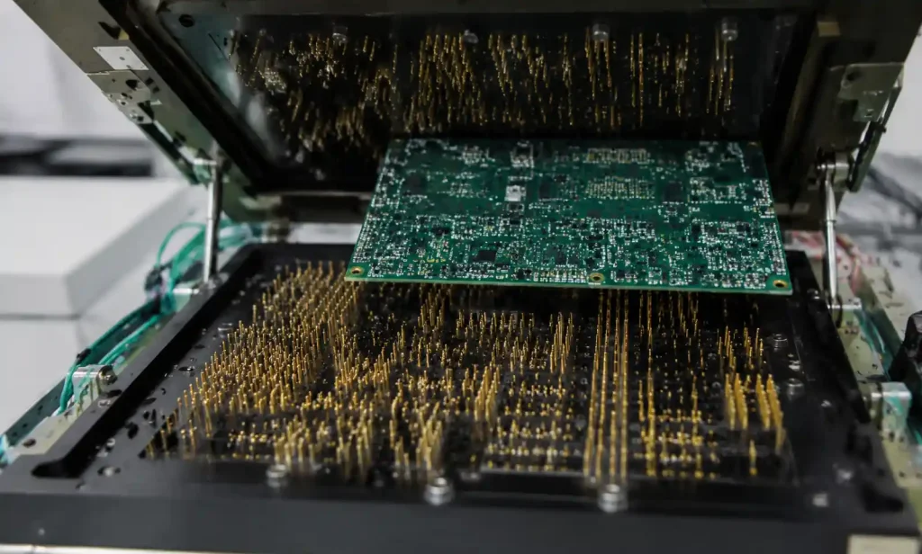
ICT is the high-volume electrical workhorse. A custom “bed of nails” fixture presses hundreds of spring-loaded pins onto dedicated test points at once, then measures every component in parallel. Once the fixture and program exist, a board tests in seconds, and coverage on a well-designed board reaches 85–98% of nets and component values.
The catch is the fixture. It is a one-time NRE of roughly $800 to several thousand dollars for a simple board, and far more for complex ones, plus it needs test-point access designed into the layout. Change the board and you often rebuild the fixture. ICT only pays off once volume amortizes that cost.
Coverage, Cost, and Speed Compared
The four methods trade fixture cost against per-board speed and against what they can actually detect. This is the core decision table.
| Method | Type | Fixture / NRE | Speed per Board | Best Volume |
|---|---|---|---|---|
| AOI | Optical inspection | None | 10–20 sec | All volumes |
| X-Ray (AXI) | Radiographic inspection | None | 1–5 min (targeted) | All, hidden joints |
| Flying Probe | Electrical, fixtureless | None | 3–8 min | Proto to ~1,000 |
| ICT | Electrical, bed-of-nails | ~$800–$10,000+ | 10–60 sec | 1,000+ |
Match that to what each method catches, because coverage gaps are where escapes happen.
| Defect | AOI | X-Ray | Flying Probe | ICT |
|---|---|---|---|---|
| Missing / wrong part | Yes | Partial | Partial | Yes |
| Solder bridge (visible) | Yes | Yes | Yes | Yes |
| Hidden BGA / QFN joint | No | Yes | No | No |
| Solder voiding | No | Yes | No | No |
| Open / short (net) | No | Partial | Yes | Yes |
| Wrong component value | No | No | Yes | Yes |
| Board functions (boots) | No | No | No | No |
No method in this table confirms the board actually works in its application. That last gap belongs to functional test (FCT), the final gate before shipment.
How to Sequence Your Test Strategy
Test strategy follows volume and risk, not habit. The order below reflects how experienced lines actually build coverage.
For prototypes and NPI, run AOI plus flying probe. You get workmanship and electrical coverage with zero tooling cost while the design is still moving. Add targeted X-ray if the board carries BGAs.
For stable production above roughly 1,000 units, the math flips: the ICT fixture NRE amortizes across the run and per-board test time collapses to seconds. AOI stays inline as process control, and X-ray covers the hidden joints ICT cannot electrically reach.
Two rules save the most money. First, design for test early: give ICT its test points and keep BGA edges accessible for X-ray, or you pay in coverage later. Second, do not over-test. Layering every method on a simple, low-volume board burns cost without lowering escape risk. Reputable PCB E-test and assembly capabilities should include the test data and reports as standard proof, not an upcharge.
FAQs
Does AOI replace X-ray inspection?
No. AOI inspects visible joints fast, but it cannot see under BGAs or QFNs. X-ray is the only method that images those hidden joints and measures internal voiding, so dense boards need both.
When is flying probe better than ICT?
For prototypes, frequent revisions, and volumes under about 1,000 boards. It needs no fixture, so it starts fast and adapts to netlist changes. ICT wins once volume amortizes its fixture cost.
What test coverage does ICT provide?
On a board designed with proper test-point access, ICT typically reaches 85–98% coverage of nets and component values. Poor access lowers that number, which is why design-for-test matters.
Do these tests confirm the board works?
No. AOI, X-ray, flying probe, and ICT verify construction and connectivity. Functional test (FCT) is the separate step that powers the board and confirms it performs its intended job.
What is the acceptable voiding limit for a BGA joint?
IPC-A-610 commonly caps voiding at 25% by area per ball, though critical applications tighten this. X-ray is the standard tool for measuring it.
Conclusion
There is no single “best” PCB test, only the right combination for your board and volume. Inspection (AOI and X-ray) proves the board is built correctly; electrical test (flying probe and ICT) proves the connections are sound. Prototypes lean on AOI plus flying probe for zero-tooling flexibility, while volume production shifts to ICT once the fixture cost amortizes, with X-ray always covering the hidden joints no camera can reach. Design for test early and match methods to risk, not habit.
Andwin Circuits builds and tests boards up to 50 layers with inline AOI, X-ray, flying probe, and ICT, delivering full test reports with fast turnaround in 7 days. Contact us today for turnkey assembly and testing with factory-direct pricing.