
PCB Cost Reduction Strategies: DFM Techniques That Save Money
PCB manufacturing accounts for 20-35% of hardware product cost, yet most design teams overlook basic DFM principles that could cut expenses by 15-40% without sacrificing quality or performance.
Your PCB budget is determined long before fabrication starts. Layer count decisions, via strategies, material choices, and panelization directly control both NRE and unit cost. A 6-layer board that could work as a 4-layer design costs 60-80% more per unit. Non-standard hole sizes force tool changes that add setup time and scrap. Specifying exotic materials when FR-4 suffices doubles laminate cost.
This guide covers the DFM techniques that deliver measurable cost savings: panel utilization optimization, layer count reduction, via minimization, standard material selection, hole size standardization, and surface finish choices. These are the levers our engineering team pulls daily to bring complex designs within budget while maintaining signal integrity and reliability.
Why DFM Drives PCB Cost
DFM (Design for Manufacturing) is the practice of designing PCBs that align with standard fabrication processes, reducing setup time, tool changes, material waste, and yield loss.
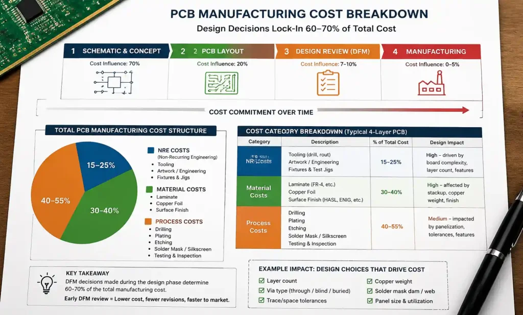
Manufacturing cost breaks into three buckets: NRE (tooling, artwork, test fixtures), material (copper-clad laminate, prepreg, surface finish), and process (drilling, plating, etching, testing time). DFM targets all three simultaneously. A board designed without DFM consideration forces custom tooling, non-standard processes, and low panel utilization, inflating cost at every stage.
According to IPC-2221 design standards, 60-70% of manufacturing cost is locked in during the design phase. Once you commit to 8 layers, 0.1mm microvias, or Rogers high-frequency material, your cost floor is set. DFM review before fabrication identifies opportunities to simplify without compromising electrical performance.
Panel Utilization: The Hidden Cost Factor
Panel utilization is the percentage of working panel area occupied by actual boards versus wasted space in rails, gaps, and scrap edges.
Standard PCB manufacturing panel sizes are 457×610mm (18×24 inches) or 305×457mm (12×18 inches). Your board dimensions determine how many units fit per panel, and poor nesting wastes expensive laminate. A 95mm × 115mm board placed haphazardly might yield 12 units per panel, but rotated 90° and tightly arrayed, the same board fits 16 units—a 33% cost reduction per board with zero design changes.
Target 75-85% panel utilization as baseline. Below 70% signals inefficient board sizing or array layout. Above 85% risks inadequate rails for PCB assembly handling. For low-volume prototypes where panel cost dominates, even adjusting board outline by 2-3mm to fit one additional unit per panel saves 8-10% per board.
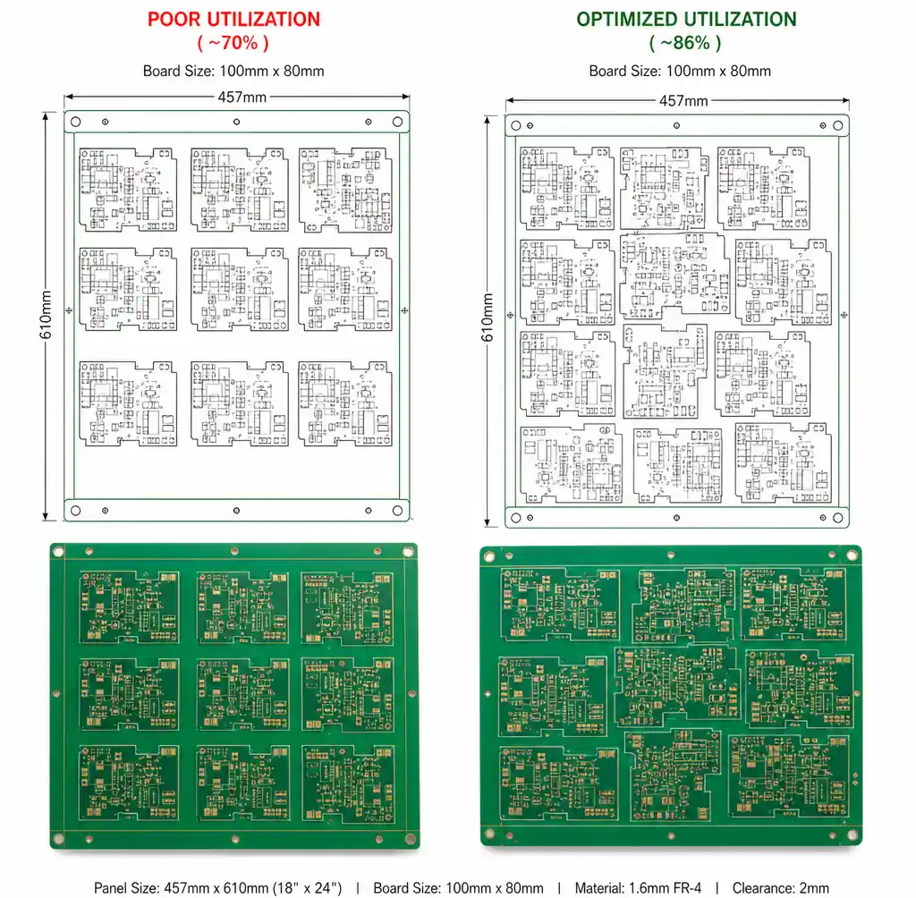
Key tactics: choose board dimensions that divide evenly into standard panels, use V-scoring for rectangular boards to eliminate spacing gaps (see PCB panelization), and consult fab utilization analysis during schematic phase, not after layout completion.
Layer Count Optimization
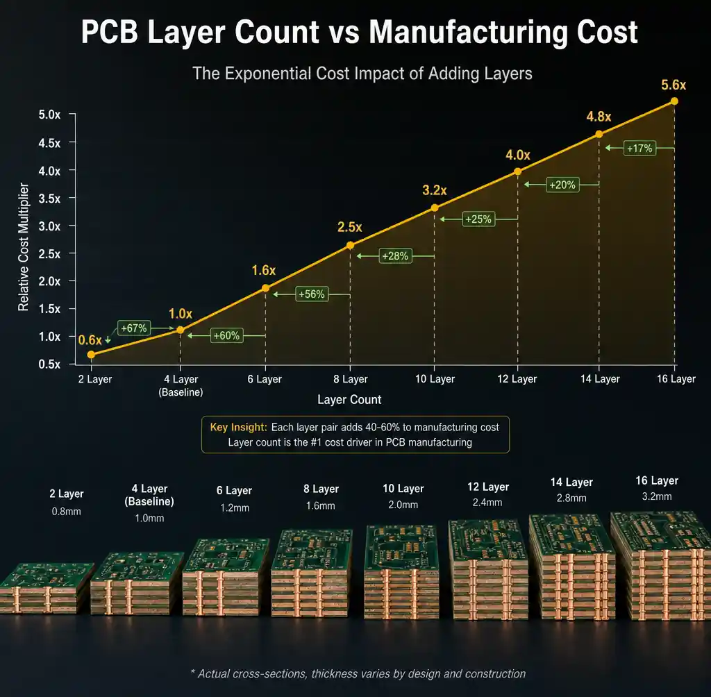
Layer count is the single largest cost lever in PCB design. Each additional layer pair increases laminate material, press cycles, and drilling complexity.
A 4-layer board costs 40-60% less than a 6-layer board of identical size. An 8-layer board costs 2-2.5× more than a 4-layer. The cost curve is exponential because high layer counts require more prepreg sheets, longer lamination cycles, tighter drilling tolerances, and additional inner-layer imaging and etching steps.
You can reduce layers without sacrificing signal integrity by applying these techniques: use both sides fully before adding layers, employ tighter trace/space rules (4mil vs 6mil frees 25-30% more routing area), leverage blind and buried vias in HDI PCB designs to route between specific layer pairs instead of adding full planes, consolidate power and ground into split planes where current draw permits, and accept slightly longer trace routes if it avoids an entire layer.
| Layer Count | Relative Cost per Board | Typical Application | Lead Time Impact |
|---|---|---|---|
| 2-layer | 1.0× (baseline) | Simple digital, power supplies | 3-5 days |
| 4-layer | 1.4-1.6× | Microcontroller, IoT | 5-7 days |
| 6-layer | 2.2-2.8× | High-speed digital, DDR3 | 7-10 days |
| 8-layer | 3.5-4.5× | DDR4, PCIe, RF | 10-14 days |
| 10+ layers | 5.0-8.0×+ | Servers, telecom, FPGA | 14-21 days |
Field example: we reviewed a client’s 8-layer IoT gateway board where four layers were less than 30% routed. By consolidating signals onto two dense layers and merging split power planes, we delivered a functionally identical 4-layer design that cut per-unit cost by 58% and shaved 5 days off lead time. The designer assumed more layers meant easier routing, but it actually meant higher cost with no performance gain.
Via Strategy and Cost Impact
Vias add cost through drilling time, copper plating, and potential yield loss, especially at small diameters.
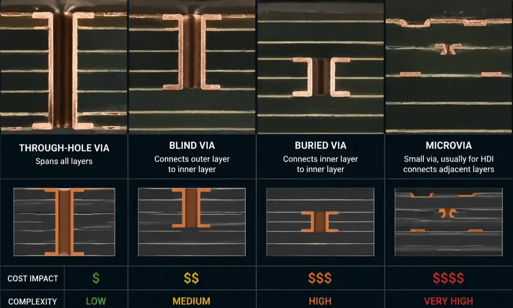
Through-hole vias (plated through the entire board) are the cheapest because they use standard drills and single-pass plating. Blind vias (outer layer to inner layer) and buried vias (inner to inner) require sequential lamination and multiple drill passes, adding 20-40% to fabrication cost but saving board area in dense HDI PCB layouts.
Reducing via count by 20-30% directly lowers drilling cost and improves yield. Tactics include: use wider traces and fewer vias for low-speed signals (power, I/O under 10 MHz), route signals on the same layer when possible instead of layer-hopping, share vias between multiple nets where design rules allow (common ground connections), and eliminate redundant vias used for “just in case” layer transitions.
Via size matters too. Standard drill sizes (0.3mm, 0.4mm, 0.5mm) are faster and cheaper than custom sizes because they require no tool changes. Requesting 0.35mm or 0.45mm vias forces the fab to swap bits mid-run, adding setup time. Microvias (laser-drilled, <0.15mm) used in HDI boards cost more per hole but enable higher density, reducing layer count—the net effect is usually cost-neutral or positive for complex designs.
| Via Type | Diameter Range | Drill Method | Relative Cost per Via | When to Use |
|---|---|---|---|---|
| Through-hole | 0.3-1.0mm | Mechanical drill | 1.0× (baseline) | Standard routing |
| Blind via | 0.2-0.5mm | Mechanical or laser | 1.3-1.5× | HDI, space-constrained |
| Buried via | 0.2-0.5mm | Mechanical or laser | 1.5-1.8× | HDI inner layers |
| Microvia (laser) | 0.1-0.15mm | Laser | 1.2-1.4× | Fine-pitch BGA, HDI |
For cost-sensitive designs, stick to through-hole vias and standard drill sizes unless board density absolutely requires HDI construction.
Standard Materials vs Custom Stackups
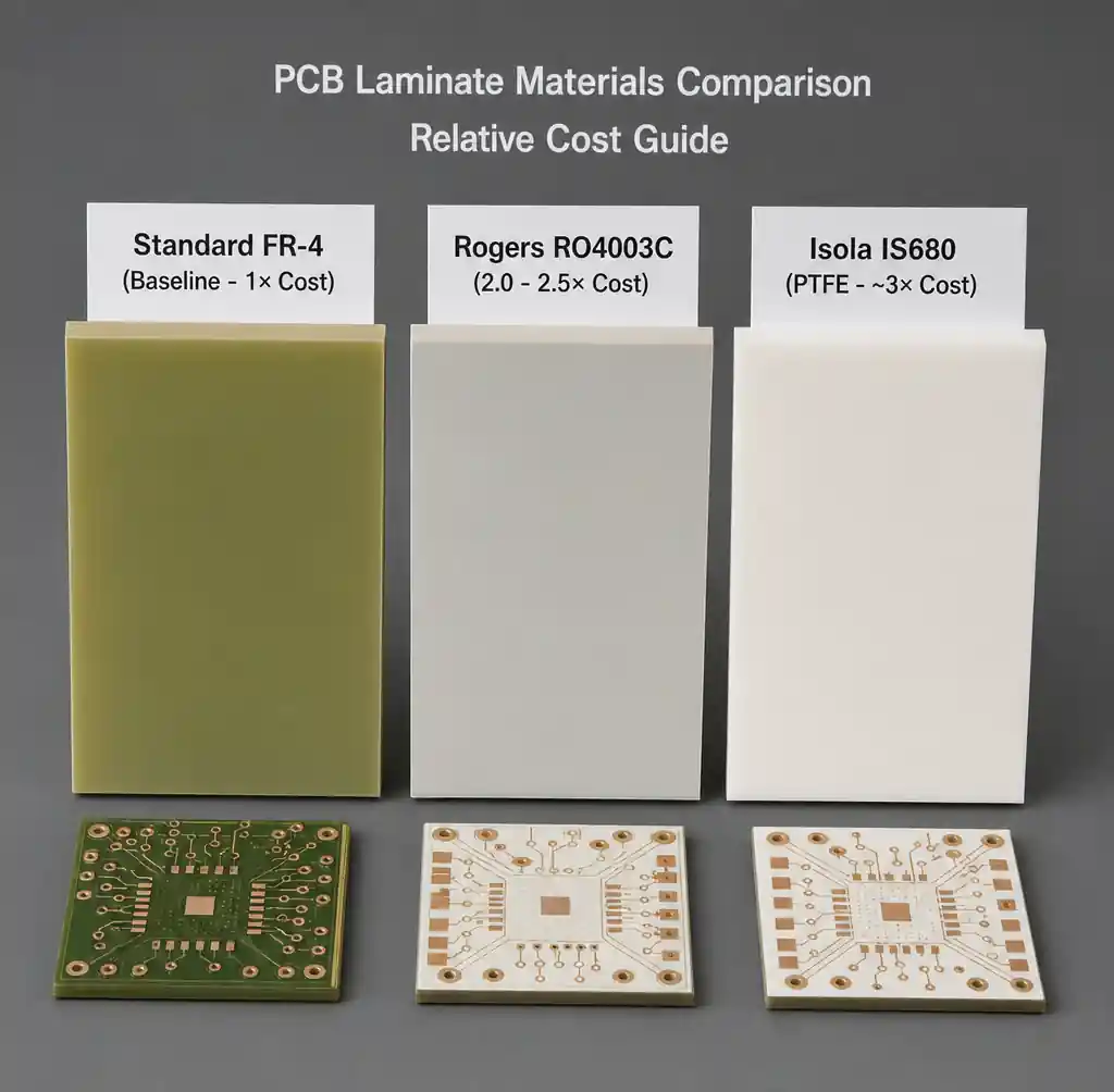
Material selection controls both laminate cost and availability, with standard FR-4 offering the best balance for 90% of applications.
FR-4 (Flame Retardant 4) is the industry baseline: glass-reinforced epoxy with Tg 130-140°C, adequate for signals up to 1-2 GHz and operating temperatures to +130°C. It costs 1× (baseline). Upgrading to high-Tg FR-4 (Tg 170-180°C) adds 10-20% material cost but improves reliability for automotive, industrial, and power electronics exposed to sustained high temperatures.
High-frequency materials (Rogers, Taconic, Isola) cost 3-6× more than FR-4 and add lead time because fabs stock less inventory. Use them only when signal integrity analysis proves FR-4 cannot meet loss or impedance tolerance at your operating frequency. For designs below 5 GHz, controlled-impedance FR-4 with proper stackup design usually suffices.
Copper weight also impacts cost. Standard 1oz (35μm) copper is baseline. Heavy copper (2oz, 3oz, 6oz) used in high-current power boards costs 20-50% more per ounce-step due to thicker plating and etching difficulty. Specify heavy copper only where current density calculations require it, and use it selectively on power layers rather than all layers.
Material cost breakdown example (4-layer, 100mm × 150mm board, 100 units):
- Standard FR-4, 1oz copper: $8-12 per board
- High-Tg FR-4, 1oz copper: $10-14 per board (+20%)
- Rogers RO4003C, 1oz copper: $28-40 per board (+250%)
- FR-4, 2oz copper: $11-16 per board (+35%)
For mixed-signal or RF boards, consider hybrid stackups: Rogers on outer layers for RF traces, FR-4 for inner power and digital layers. This cuts material cost 40-50% versus all-Rogers construction while preserving RF performance.
Hole Size Standardization
Drill bit changes during fabrication add non-value time and increase cost. Each unique hole size requires a tool swap, depth calibration, and hit verification.
Standard drill sizes (in mm: 0.25, 0.30, 0.35, 0.40, 0.50, 0.60, 0.80, 1.00, 1.20) are faster because fabs pre-load them and optimize drill programs around common sizes. Using 8-10 standard sizes versus 15-20 custom sizes can reduce drilling cost by 10-15% on complex boards.
Component selection drives hole size. When choosing through-hole connectors, switches, and terminal blocks, prioritize parts with standard lead diameters (0.6mm, 0.8mm, 1.0mm) that use common drill sizes. Avoid parts with odd lead pitches or diameters (0.65mm, 0.75mm, 0.95mm) unless functionally critical.
For via holes, stick to 0.3mm or 0.4mm finished hole size (0.5mm or 0.6mm drill before plating). These sizes offer good current carrying capability and reliable plating without forcing custom tooling.
Standardization extends to annular rings (copper pad around the hole). IPC-6012 Class 2 requires minimum 50μm annular ring; Class 3 requires 75μm. Design to Class 2 tolerances unless reliability requirements demand Class 3, because tighter tolerances reduce yield and raise cost by 8-12%.
Surface Finish Selection for Cost
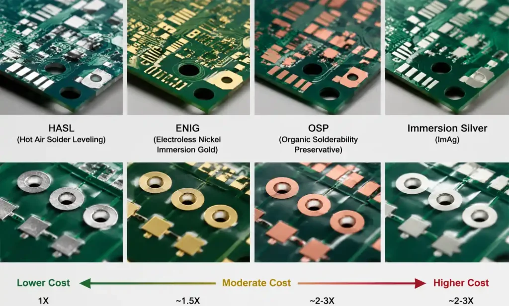
Surface finish protects exposed copper and provides a solderable surface. Cost and shelf life vary significantly across finish types.
HASL (Hot Air Solder Leveling) is the cheapest option at baseline cost, suitable for through-hole and standard SMT assembly. Lead-free HASL adds 5-10% cost. HASL leaves an uneven surface (±1-2 mil variation) unsuitable for fine-pitch BGAs below 0.5mm pitch.
ENIG (Electroless Nickel Immersion Gold) costs 30-50% more than HASL but delivers flat surface for fine-pitch parts, longer shelf life (12+ months), and better contact reliability for edge connectors and test points. Use ENIG for HDI PCB, BGA assemblies, and products with long storage before assembly.
OSP (Organic Solderability Preservative) costs 10-20% more than HASL, provides flat surface, but has shorter shelf life (3-6 months) and only one reflow cycle. OSP works well for high-volume production with quick turnaround from fab to assembly, but avoid it for prototypes or low-volume builds with uncertain assembly schedules.
| Surface Finish | Relative Cost | Surface Flatness | Shelf Life | Best Application |
|---|---|---|---|---|
| HASL (leaded) | 1.0× (baseline) | Uneven (±1-2 mil) | 6-12 months | Through-hole, standard SMT |
| HASL (lead-free) | 1.1× | Uneven (±1-2 mil) | 6-12 months | RoHS compliance, standard SMT |
| ENIG | 1.3-1.5× | Flat (±0.2 mil) | 12+ months | Fine-pitch BGA, HDI, edge connectors |
| OSP | 1.1-1.2× | Flat | 3-6 months | High-volume, fast turnaround |
| Immersion Silver | 1.2-1.3× | Flat | 6-9 months | Aluminum wire bonding, RF |
For cost-sensitive designs, use HASL for prototypes and pilot runs, then switch to ENIG for production if you have fine-pitch components. For boards without BGAs or QFNs, HASL or lead-free HASL keeps cost lowest.
Volume Discounts and MOQ Planning
PCB fabrication cost per board drops significantly with volume due to setup amortization and material purchasing scale.
NRE (tooling, artwork, test fixtures) is fixed per design revision, typically $200-800 depending on complexity. At 10 units, NRE adds $20-80 per board. At 1,000 units, NRE adds $0.20-0.80 per board—negligible. This is why prototype quantities (5-25 boards) cost 3-5× more per unit than production volumes (500-5,000 boards).
Material and fabrication also scale. Fabs optimize panel layout for higher volumes, negotiate better laminate pricing, and run longer production batches with fewer setups. Typical volume breaks:
- 1-10 units: Prototype pricing, minimal optimization
- 25-100 units: Low-volume production, some panel optimization
- 100-500 units: Production pricing, optimized panelization
- 500-5,000 units: Volume discount tier 1 (15-25% off 100-unit price)
- 5,000+ units: Volume discount tier 2 (25-40% off 100-unit price)
Strategic volume planning: if your annual forecast is 2,000 boards spread across four orders of 500 units, consolidate into two orders of 1,000 units to jump a discount tier. This requires holding inventory but can save 10-15% total. For consigned inventory programs where the fab holds stock and releases on demand, you capture volume pricing without carrying cost.
Assembly follows similar curves. PCB assembly setup (stencil, program, feeder loading) is fixed per design. At 10 boards, setup might cost $8-15 per board. At 500 boards, setup cost drops to $0.15-0.30 per board. Plan pilot runs at minimum MOQ (often 25-50 units), then commit to production volume once design is validated.
Real Cost Comparison: Optimized vs Unoptimized Design
Here is a side-by-side cost breakdown for an IoT controller board designed two ways: baseline (unoptimized) and DFM-optimized, at 500-unit production volume.
| Design Element | Unoptimized Design | DFM-Optimized Design | Cost Impact |
|---|---|---|---|
| Layer count | 6 layers (low utilization) | 4 layers (dense routing) | -42% material cost |
| Board size | 105mm × 125mm (poor nesting) | 100mm × 120mm (optimized) | +12% panel utilization |
| Via count | 450 vias (mixed sizes) | 320 vias (standard sizes) | -15% drilling cost |
| Material | High-Tg FR-4 (unnecessary) | Standard FR-4 (sufficient) | -18% laminate cost |
| Surface finish | ENIG (no fine-pitch parts) | HASL lead-free (adequate) | -35% finish cost |
| Hole sizes | 18 unique drill sizes | 8 standard drill sizes | -12% drilling time |
| Unit cost (500 pcs) | $24.50 per board | $14.80 per board | -40% total cost |
The optimized design delivers identical electrical performance, same component selection, and same form factor (within 5% board area). The savings come entirely from aligning design choices with standard fabrication processes. At 500 units, this is $4,850 saved. At 5,000 units annual volume, it is $48,500 saved—enough to fund two additional engineering projects.
FAQs
What is the quickest way to reduce PCB cost?
Reduce layer count if utilization is below 70% on existing layers, then optimize panel layout for better nesting. These two changes alone typically save 20-35% without redesign.
How much does switching from 6 layers to 4 layers save?
A 4-layer board costs 40-60% less than a 6-layer board of the same size. Exact savings depend on board dimensions, copper weight, and volume, but expect $8-15 per board reduction at 500-unit volumes.
Should I use HDI vias to reduce cost?
HDI (microvias, blind/buried vias) costs more per via but enables higher routing density, potentially reducing layer count. For dense boards (BGA, >0.5mm pitch), HDI can lower total cost by eliminating 2-4 layers. For simple boards, stick to through-hole vias.
Is Rogers material always necessary for RF designs?
No. For frequencies below 3-5 GHz, controlled-impedance FR-4 often meets loss and impedance tolerance. Rogers and other high-frequency laminates are needed for >10 GHz, tight loss budgets, or millimeter-wave designs. Use controlled impedance PCB design principles on FR-4 first.
How does surface finish affect assembly cost?
ENIG and OSP provide flat surfaces required for fine-pitch BGAs (<0.5mm pitch). HASL is adequate for standard SMT (≥0.5mm pitch) and through-hole. Using HASL instead of ENIG saves 30-50% on finish cost when fine-pitch parts are not present.
Can I mix materials to save cost?
Yes. Hybrid stackups use high-frequency material on outer layers for RF traces and FR-4 on inner layers for power and digital. This cuts material cost 40-50% versus all-Rogers construction while maintaining RF performance. Discuss hybrid stackup with your fab during DFM review.
What is a reasonable panel utilization target?
Target 75-85% utilization for production volumes. Below 70% wastes laminate; above 85% risks inadequate rails for assembly handling. Adjust board outline dimensions by 2-5mm if it significantly improves nesting.
Conclusion
PCB cost reduction is not about cutting corners—it is about designing smarter from the start. The techniques in this guide (panel utilization optimization, layer count reduction, standard material selection, via minimization, and hole size standardization) cut manufacturing cost by 20-40% while maintaining signal integrity, reliability, and compliance with industry standards. Apply DFM principles during schematic and layout, not after fabrication quotes come back high.
If you need expert DFM review and cost optimization for your next PCB project, Andwin Circuits offers advanced manufacturing capabilities up to 50 layers with fast delivery in 7 days. Our engineering team provides complimentary DFM analysis, material selection guidance, and panelization optimization backed by ISO 9001 and IATF 16949 certification. We have delivered cost-optimized PCBs for automotive, medical, IoT, and telecommunications applications worldwide.
Contact us today for custom PCB solutions, DFM consultation, and competitive factory-direct pricing.