
PCB Manufacturing in China vs Other Countries: Cost and Quality Comparison
If you want to select the right PCB manufacturing location for your electronics project, then you will need to understand cost structures, quality standards, lead times, and technical capabilities across different manufacturing regions that directly impact your product’s profitability and time-to-market.
China produces over 60% of global PCB output, while the United States, Europe, and other Asian countries maintain specialized manufacturing segments. Production cost differences reach 30-50% between regions, but total landed costs including tariffs, shipping, and quality risks present a more complex decision framework. Hardware engineers and sourcing managers face increasing pressure to balance cost efficiency with quality assurance, intellectual property protection, and supply chain resilience.
This comprehensive comparison analyzes PCB manufacturing across major production regions, providing data-driven insights into cost structures, quality capabilities, lead time performance, and strategic considerations for electronics manufacturers.
Global PCB Manufacturing Landscape
The global PCB manufacturing industry concentrates in specific regions, each offering distinct advantages in cost, technology, and market access. Understanding regional strengths helps optimize sourcing decisions.
China PCB Manufacturing Dominance
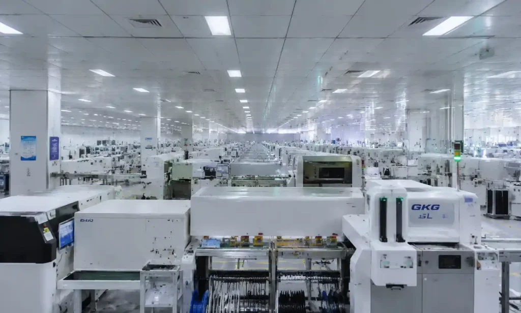
China controls 60% of global PCB production by value, supported by concentrated supply chains in Guangdong and Jiangsu provinces. The Shenzhen-Dongguan-Huizhou industrial corridor hosts over 1,500 PCB manufacturers ranging from basic single-layer board shops to advanced HDI PCB and rigid flex PCB facilities producing boards up to 50 layers.
Chinese manufacturers invested heavily in automation and advanced equipment from 2015-2025, closing the technology gap with Western facilities. Top-tier Chinese factories now operate the same Schmoll laser drilling systems, Burkle lamination presses, and Orbotech AOI equipment found in North American and European plants. This equipment parity, combined with lower labor costs and supply chain density, creates substantial cost advantages while maintaining comparable technical capabilities for most applications.
North American Manufacturing Position
The United States maintains approximately 5% of global PCB production, focused on high-reliability applications, quick-turn prototyping, and defense sector requirements. Domestic manufacturers serve aerospace, military, medical device, and ITAR-regulated projects where security, compliance, or rapid iteration outweigh cost considerations.
North American facilities excel in engineering support, IP protection, and regulatory compliance but operate with 200-300% higher labor costs. The domestic PCB industry consolidated significantly from 2000-2020, leaving approximately 150 manufacturers concentrated in California, Colorado, New York, and Minnesota.
European PCB Manufacturing
Europe produces roughly 3% of global PCB output, concentrated in Germany, Austria, and France. European manufacturers specialize in automotive electronics, industrial control systems, and medical devices requiring strict quality control and full traceability. Strong automotive industry relationships and proximity to major OEMs support specialized capabilities in automotive PCB and high-reliability applications.
European facilities operate under stringent environmental regulations (REACH, RoHS) and maintain comprehensive documentation systems. Labor costs exceed North American levels, but manufacturers compete through technical specialization, rapid response, and integrated design services.
Other Asian Manufacturing Regions
Taiwan, South Korea, and Japan maintain significant PCB capabilities focused on advanced technology and high-margin products. Taiwan dominates IC substrate and high-layer-count HDI production for semiconductor packaging. South Korea leads in flexible PCB for consumer electronics displays. Japan specializes in high-frequency materials and ultra-precise fabrication for RF and microwave applications.
These regions offer middle-ground positioning: higher costs than China but lower than Western manufacturers, with strong technical capabilities in specialized product segments.
Cost Comparison Analysis
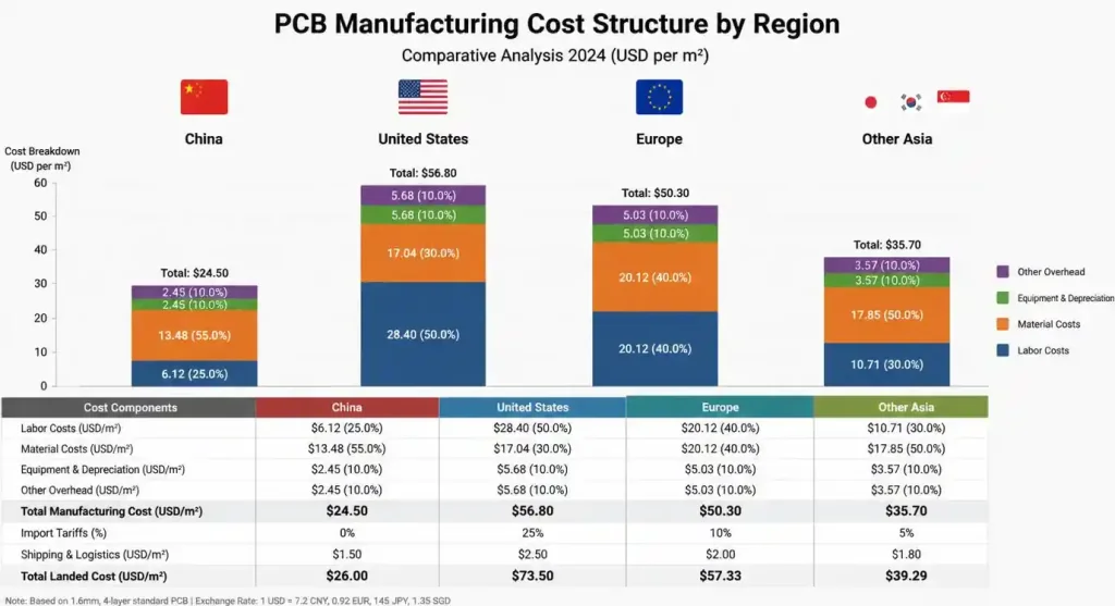
Cost structures vary significantly across manufacturing regions due to labor rates, material sourcing, equipment utilization, and overhead factors. Total landed cost analysis reveals the actual economic differences.
| Cost Factor | China | United States | Europe | Other Asia |
|---|---|---|---|---|
| Base Fab Cost | Baseline | +150-200% | +180-220% | +40-80% |
| Assembly Cost | Baseline | +200-300% | +220-280% | +60-100% |
| Labor Component | 15-20% | 45-55% | 50-60% | 25-35% |
| Material Premium | Baseline | +10-15% | +15-20% | +5-10% |
| Lead Time | 7-15 days | 3-10 days | 10-18 days | 8-14 days |
China Manufacturing Cost Structure
Chinese PCB manufacturing base costs run 30-50% lower than North American equivalents for comparable specifications. A standard 6-layer multilayer PCB measuring 100mm × 150mm costs approximately $12-18 per piece in China for production volumes of 100-500 units, compared to $35-50 in the United States.
This cost advantage stems from multiple factors: labor costs averaging $4-7 per hour versus $25-40 in North America, concentrated supply chains reducing material costs by 15-25%, higher equipment utilization rates (85-95% versus 60-75% in Western facilities), and lower facility overhead due to regional industrial clustering. The Guangdong supply chain allows manufacturers to source FR4 laminates, copper foil, solder mask, and specialty materials within 50km, minimizing inventory carrying costs and enabling just-in-time production.
However, 2025-2026 tariff increases impact total landed costs. Current Section 301 tariffs of 25% plus additional 10% duties apply to most PCB imports into the United States. For the example 6-layer board, tariffs add $4.20-6.30 per piece, bringing China-sourced total cost to $16.20-24.30 versus $35-50 domestic production. Net savings of 32-54% persist even after tariffs for production volumes exceeding 100 units.
North American Cost Structure
US PCB manufacturing carries substantially higher base costs but eliminates tariffs, reduces shipping expenses, and shortens supply chain risks. Labor represents 45-55% of total cost versus 15-20% in China. A PCB assembler in California earning $28-35 per hour plus benefits ($42-52 total compensation) performs the same work as a Shenzhen assembler earning $5-8 per hour total compensation.
Material costs run 10-15% higher due to smaller purchasing volumes and limited domestic supply chains. Most US manufacturers import FR4 laminates, specialty substrates, and surface finish chemicals, adding cost and lead time. Equipment depreciation costs are higher due to lower utilization rates – a $2 million laser drilling system running at 65% capacity costs more per panel than the same machine at 90% capacity.
The cost premium makes economic sense for specific scenarios: ITAR compliance requirements, volumes under 50-100 units where setup costs dominate, projects requiring rapid iteration (24-72 hour prototyping), and applications where IP security justifies premium pricing. For quick turn PCB assembly needs under one week, domestic sourcing often provides better total economics.
Total Landed Cost Calculation
Smart sourcing decisions require total landed cost analysis, not just base pricing comparison. Key factors include:
Tariffs and Duties: Current 35% combined tariff on Chinese PCBs significantly narrows the cost gap. A $15 China-sourced board becomes $20.25 landed cost before freight.
Freight and Logistics: Air freight from China adds $0.50-2.00 per board depending on size and weight, plus customs clearance fees of $150-300 per shipment. Ocean freight reduces per-unit costs but extends lead times by 4-6 weeks.
Inventory Carrying Costs: Longer lead times require larger safety stock. A 30-day China supply chain versus 5-day domestic sourcing impacts working capital requirements significantly for production volumes.
Quality Risk Costs: Defect rates vary by manufacturer quality tier, not just geography. However, rework logistics are more complex and expensive with offshore sourcing. A 2% defect rate requiring air freight returns and replacement adds $3-5 per defective unit in logistics costs alone.
Quality Standards and Certifications
Quality capabilities depend on individual manufacturer implementation of standards, not geographic location alone. However, regional certification patterns and enforcement rigor vary significantly.
IPC Standards Compliance
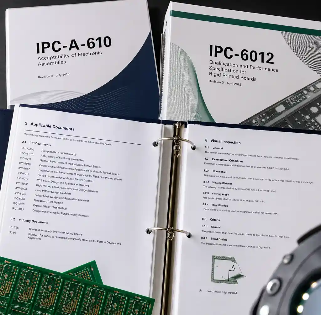
IPC standards define global PCB quality benchmarks. IPC-6012 establishes performance specifications for rigid PCBs, while IPC-A-610 defines acceptance criteria for electronic assemblies. Three quality classes serve different applications:
| IPC Class | Application | Typical Industries | Defect Tolerance |
|---|---|---|---|
| Class 1 | General electronics | Consumer products | Cosmetic defects acceptable |
| Class 2 | Dedicated service | Computers, telecommunications | Limited imperfections allowed |
| Class 3 | High reliability | Medical, aerospace, military | Zero defects, full traceability |
Chinese manufacturers routinely achieve IPC Class 2 compliance, while top-tier facilities like Andwin Circuits maintain IPC Class 3 capabilities with full documentation and traceability systems. The key differentiator is not capability to meet standards, but consistency of execution and quality management system rigor.
Western manufacturers typically enforce stricter internal process controls and inspection criteria beyond minimum IPC requirements. A Class 2 board from a German automotive supplier may exceed the actual quality of a Class 3 board from a lower-tier Chinese manufacturer, despite similar certification claims.
Industry-Specific Certifications
Industry certifications indicate specialized quality management systems and process controls for demanding applications:
IATF 16949 (Automotive): Automotive PCB manufacturers require IATF 16949 certification, which extends ISO 9001 with automotive-specific requirements including PPAP documentation, FMEA analysis, and continuous improvement systems. Major Chinese manufacturers serving automotive OEMs maintain IATF 16949 certification with identical rigor to Western suppliers. Andwin Circuits holds IATF 16949 certification for automotive applications including EV power electronics and ADAS systems.
ISO 13485 (Medical Devices): Medical device PCB manufacturing requires ISO 13485 quality management systems with full traceability, risk management, and regulatory compliance documentation. Both Chinese and Western manufacturers serving medical OEMs maintain equivalent certification levels. The differentiator is audit frequency and regulatory body relationships rather than capability.
AS9100 (Aerospace): Aerospace PCB manufacturing demands AS9100 certification with stringent configuration management and traceability. This segment remains concentrated in North American and European facilities due to ITAR restrictions and established aerospace supplier relationships, though Chinese manufacturers increasingly pursue AS9100 for commercial aerospace applications.
Quality Control Infrastructure
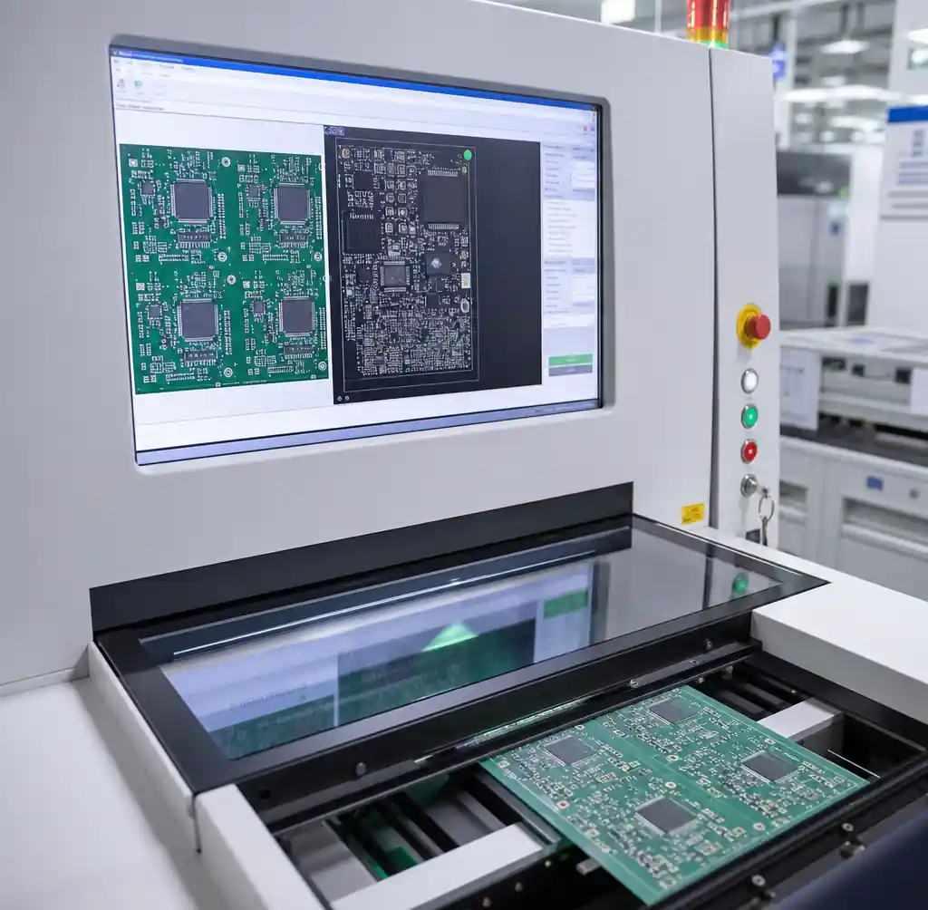
Modern PCB quality control relies on automated inspection systems regardless of manufacturing location. Automated Optical Inspection (AOI), X-ray inspection, flying probe testing, and in-circuit testing equipment costs $200,000-2,000,000 per system. Top-tier manufacturers in any region operate equivalent inspection infrastructure.
The quality differentiator is inspection criteria enforcement and corrective action systems. A Chinese manufacturer running the same Mirtec AOI system as a US manufacturer may program different defect thresholds or bypass operators may override reject signals under production pressure. Quality audits should verify not just equipment presence but actual operational procedures, reject rate tracking, and continuous improvement processes.
Technical Capabilities Comparison
Technical manufacturing capabilities increasingly converge across regions for mainstream PCB technologies. Specialized capabilities remain geographically concentrated based on historical development and application focus.
Layer Count and Complexity
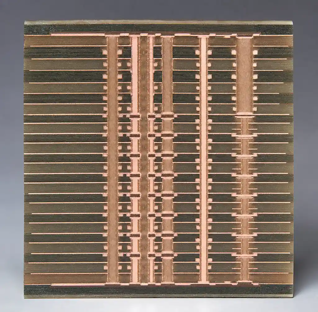
Standard multilayer PCB production (4-16 layers) is globally commoditized with equivalent capabilities across manufacturing regions. China, North America, Europe, and other Asian manufacturers routinely produce 12-layer boards with 4/4 mil trace/space, blind/buried vias, and controlled impedance to identical specifications.
High-layer-count manufacturing (20-50 layers) concentrates in specialized facilities globally. Andwin Circuits maintains production capabilities up to 50 layers with sequential lamination processes, serving high-speed computing, telecommunications infrastructure, and advanced industrial control applications. Comparable capabilities exist in Taiwan (for IC substrates), Japanese facilities (for high-frequency applications), and select North American manufacturers (for aerospace and defense). The key is identifying which specific manufacturers maintain these capabilities rather than assuming regional competence.
HDI and Advanced Technologies
HDI PCB manufacturing with laser-drilled microvias, stacked and staggered via configurations, and ultra-fine pitch patterns (3/3 mil or finer) requires specialized equipment and process expertise. This technology is globally available but implementation quality varies significantly.
Chinese manufacturers invested heavily in HDI capabilities from 2015-2025, deploying Schmoll, Mitsubishi, and ESI laser drilling systems. Current Chinese HDI production quality matches international standards for consumer electronics, IoT devices, and industrial applications. North American and European manufacturers maintain advantages in most demanding HDI applications requiring tightest tolerances and highest reliability.
Taiwan dominates the most advanced HDI segment (any-layer HDI for smartphone mainboards and IC substrates) with specialized capabilities exceeding other regions. For mainstream HDI applications, manufacturer selection should focus on specific factory audits and sample qualification rather than geographic assumptions.
Rigid-Flex and Specialty PCBs
Rigid flex PCB manufacturing requires specialized expertise in polyimide processing, controlled depth routing, and flexible circuit design rules. This technology is globally available but concentrated in facilities with dedicated rigid-flex production lines.
Chinese manufacturers increasingly dominate rigid-flex production for consumer electronics and IoT wearables. Japanese and Korean manufacturers lead in ultra-thin flexible circuits for smartphone displays and camera modules. North American and European rigid-flex specialists serve medical device and aerospace applications requiring highest reliability and full traceability.
Metal core PCB (MCPCB) for LED and power electronics applications concentrates in China due to supply chain integration with LED manufacturing clusters. Chinese MCPCB production quality and capabilities equal or exceed Western alternatives for most applications. Specialized high-thermal-conductivity substrates and ceramic PCB technologies remain more readily available from Japanese and European specialty material suppliers.
Lead Time and Delivery Performance
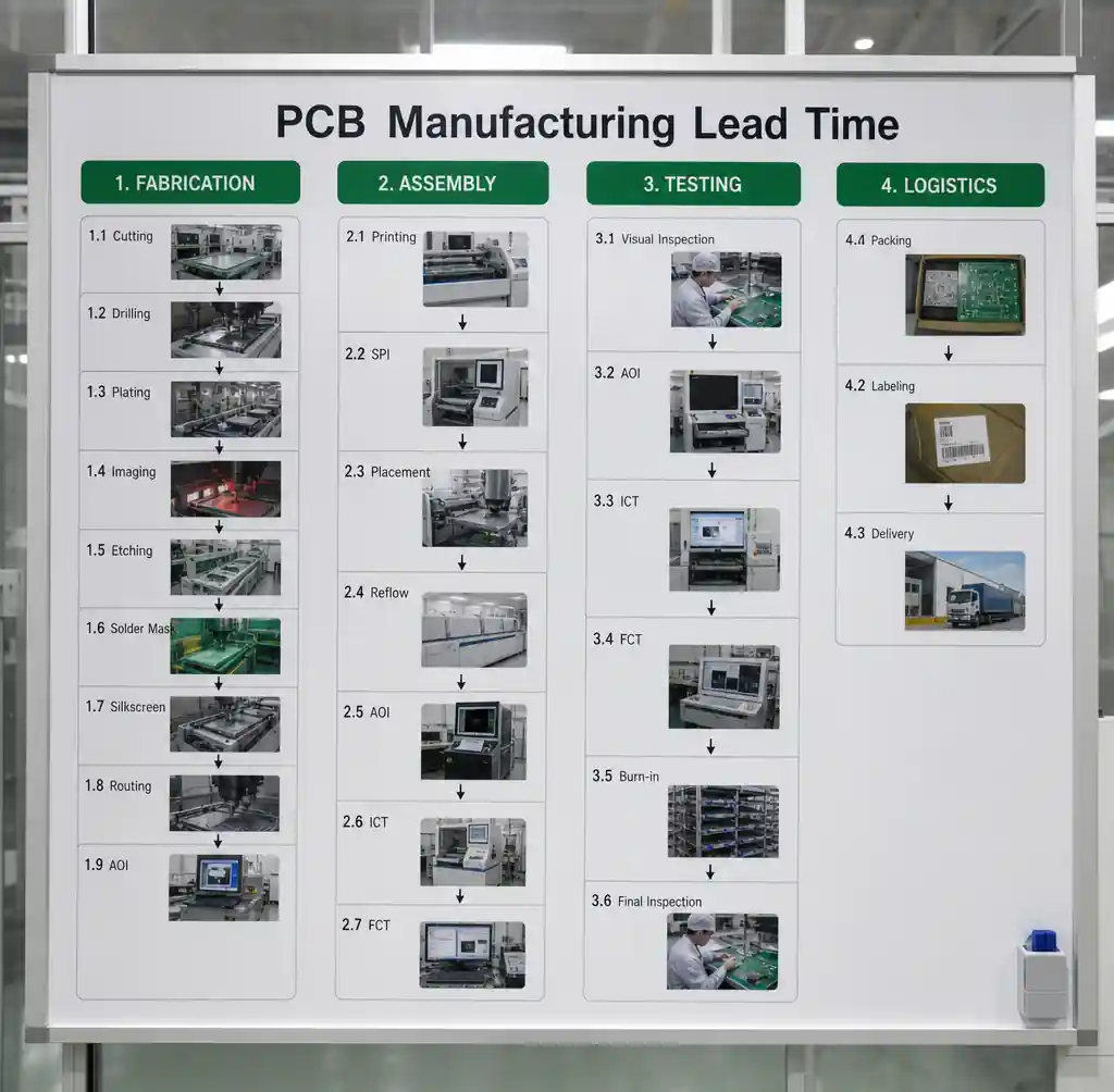
Manufacturing lead times significantly impact product development velocity and inventory management. Lead time advantages vary by project phase and volume requirements.
| Project Phase | China Lead Time | US Lead Time | Europe Lead Time | Total Transit |
|---|---|---|---|---|
| Prototype (2-4 layer) | 3-5 days fab | 24-72 hours fab | 3-7 days fab | +3-5 days China |
| Production (6-8 layer) | 7-12 days fab | 5-10 days fab | 10-15 days fab | +3-5 days China |
| Complex (10+ layer) | 10-18 days fab | 7-15 days fab | 15-22 days fab | +3-5 days China |
| Assembly | +3-7 days | +2-5 days | +5-10 days | Included above |
Prototype Development Lead Times
Quick-turn prototyping favors domestic or regional sourcing where engineering iteration speed outweighs cost considerations. North American manufacturers routinely deliver simple 2-4 layer prototypes in 24-72 hours, enabling rapid design iteration cycles. Andwin Circuits offers 7-day fast delivery for prototypes including complex multilayer PCB structures up to 50 layers, providing competitive lead times for China-sourced boards.
Total cycle time including shipping narrows geographic differences. A 3-day Chinese prototype with 4-day DHL express shipping (7 days total) compares favorably to a 5-day domestic prototype (5 days total) when cost savings reach 40-60%. The decision point shifts based on iteration frequency: projects requiring weekly respins favor domestic sourcing, while projects with 2-3 week design cycles can effectively utilize Chinese manufacturers.
Production Volume Lead Times
Production lead times for volumes exceeding 100-500 units favor Chinese manufacturing due to capacity availability and supply chain responsiveness. Chinese PCB manufacturers maintain higher equipment utilization and more flexible scheduling, allowing faster production starts. A 6-8 layer production order typically begins fabrication within 2-3 days in China versus 5-7 days in domestic facilities with higher capacity utilization.
Total production cycle times including fabrication, assembly, testing, and logistics range from 12-20 days for China-sourced production versus 8-15 days domestically. The 4-5 day differential decreases as volume increases and air freight becomes less cost-effective. For production volumes exceeding 1,000 units, ocean freight lead times of 25-35 days become economical, making absolute fabrication lead time differences less critical.
Supply Chain Reliability
Lead time consistency and on-time delivery performance vary more by individual manufacturer than by geography. However, supply chain risk profiles differ significantly. Chinese manufacturing faces potential disruption from trade policy changes, pandemic-related factory shutdowns, and logistics bottlenecks at major ports. Domestic manufacturing reduces these risks but faces material supply constraints and capacity limitations during demand surges.
Best practice supply chain management implements dual-sourcing strategies: Chinese manufacturers for production volumes with cost optimization, domestic manufacturers for rapid prototyping and supply chain backup capacity. This approach balances cost efficiency with supply chain resilience.
Supply Chain and Material Sourcing
Regional material availability and supply chain integration significantly impact manufacturing cost, lead times, and capabilities. Concentrated supply chains enable cost advantages and technical flexibility.
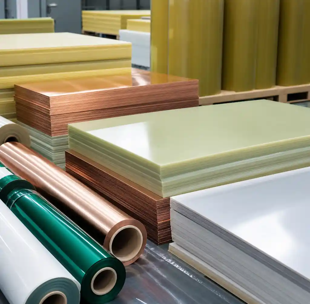
China Supply Chain Advantages
The Guangdong PCB supply chain represents the world’s most concentrated electronics manufacturing ecosystem. A Shenzhen PCB manufacturer accesses FR4 laminates from Shengyi Technology or Kingboard within 30km, surface finish chemicals from Atotech or MacDermid within the region, and solder mask from Taiyo within one-day delivery. This supply chain density enables just-in-time material sourcing, reducing inventory carrying costs by 40-60% compared to Western manufacturers.
Component sourcing for PCB assembly services similarly benefits from regional concentration. Shenzhen’s Huaqiangbei electronics market and major distributors (Arrow, Avnet, WPG) maintain massive local inventory, enabling rapid component sourcing for prototypes and production. This supply chain integration allows Chinese manufacturers to quote and produce assembled boards faster than Western competitors relying on global distribution networks.
Material cost advantages of 15-25% stem from purchasing volume and supply chain proximity rather than quality differences. Chinese PCB manufacturers consume the same Isola, Shengyi, and Panasonic materials as Western facilities, but purchase in larger volumes with lower logistics costs.
Western Supply Chain Constraints
North American and European PCB manufacturers face constrained material supply chains. Most advanced laminates and specialty materials are imported, adding 10-15% cost and extending lead times. Domestic FR4 production exists but serves limited standard grades. High-Tg materials, halogen-free laminates, and specialty substrates typically ship from Asian suppliers with 2-4 week lead times.
Component availability favors Western manufacturers for certain applications. US manufacturers access broader inventory of military-grade, automotive-qualified, and industrial-temperature components through domestic distribution. ITAR-controlled components are only available to US facilities with proper security clearances.
The material supply constraint creates a strategic disadvantage for Western PCB manufacturers competing on standard products but enables differentiation for specialized applications requiring Western-sourced materials or components.
Intellectual Property and Compliance
IP protection and regulatory compliance considerations significantly impact manufacturing location decisions for certain product categories and companies. Risk assessment requires understanding both legal frameworks and practical enforcement.
IP Protection Considerations
Intellectual property concerns remain the most cited reason for avoiding Chinese manufacturing, despite increasing legal protections. Chinese patent law strengthened significantly from 2010-2025, with specialized IP courts in Beijing, Shanghai, and Guangzhou demonstrating more consistent enforcement. However, practical IP protection depends heavily on manufacturer selection and contract terms rather than legal frameworks alone.
Best practices for IP protection with Chinese manufacturers include: requiring comprehensive non-disclosure agreements with specific damages clauses, working with established manufacturers with international customer bases and reputation risk sensitivity, limiting design file sharing to only essential manufacturing data (Gerber files without source design files), implementing design obfuscation techniques (separating critical circuits across multiple boards), and maintaining regular audit rights in manufacturing agreements.
Domestic manufacturing eliminates cross-border IP risks but does not ensure absolute protection. Former employees, shared contract manufacturers, and supply chain partners present IP risks regardless of manufacturing location. For products with truly critical IP, consider segregating sensitive components to domestic assembly with commodity PCBs sourced offshore.
Regulatory and Compliance Requirements
ITAR (International Traffic in Arms Regulations) and EAR (Export Administration Regulations) strictly control defense and dual-use technology manufacturing locations. PCBs for military, aerospace, and certain telecommunications applications must be domestically produced with documented supply chains and facility security. These requirements are non-negotiable and eliminate offshore manufacturing options entirely.
Medical device manufacturing (FDA 21 CFR Part 820) and automotive (IATF 16949) regulations are geography-neutral but require equivalent quality management systems regardless of location. Chinese manufacturers serving global medical and automotive OEMs maintain identical documentation, traceability, and process controls as Western facilities. Regulatory compliance depends on individual manufacturer audit results rather than manufacturing location.
Environmental compliance (REACH, RoHS, conflict minerals) applies equally to all manufacturers serving European and North American markets. Chinese manufacturers exporting to these markets maintain equivalent compliance programs, often using the same third-party testing laboratories (SGS, TÜV, UL) as Western manufacturers.
Strategic Decision Framework
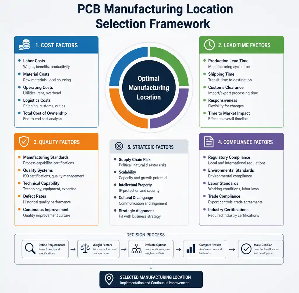
Manufacturing location decisions should follow structured analysis of project requirements, volume economics, and strategic priorities rather than geography-based assumptions. Different project phases and product categories optimize to different sourcing strategies.
| Decision Factor | Favor China | Favor Domestic | Favor Other Asia |
|---|---|---|---|
| Volume | >100-500 units | <100 units | Medium runs 500-2000 |
| Lead Time Priority | Moderate (2-3 weeks OK) | Critical (<1 week) | Moderate (1-2 weeks) |
| Cost Sensitivity | High (cost optimization) | Low (performance priority) | Medium |
| IP Sensitivity | Standard designs | Critical IP | Moderate |
| Compliance | Commercial products | ITAR/defense required | Automotive specialty |
| Technical Complexity | Standard to advanced | Cutting-edge or specialty | High-end consumer |
Prototype Phase Strategy
Development prototyping prioritizes iteration speed over cost. For projects requiring weekly or bi-weekly respins, domestic manufacturing delivers 2-3 day total advantage per iteration, accelerating time-to-market by 4-8 weeks over a typical 6-12 month development cycle. This time advantage often justifies 50-100% cost premiums for prototype quantities of 5-25 units.
Projects with longer iteration cycles (3-4 weeks) can effectively utilize Chinese manufacturers offering 7-10 day lead times including shipping. Andwin Circuits provides fast turnaround in 7 days for multilayer PCB prototypes, offering competitive lead times with substantial cost savings for development budgets.
Production Volume Strategy
Production economics favor Chinese manufacturing for most commercial applications once volumes exceed 100-500 units. The volume threshold where cost savings justify longer lead times depends on product margins: low-margin consumer products shift offshore at lower volumes (50-100 units), while high-margin industrial and medical products may source domestically up to 500-1000 units to minimize supply chain complexity.
Best practice implements progressive sourcing: prototypes domestic for speed, pre-production runs (50-200 units) Chinese manufacturers to validate offshore supply chain and quality, production volumes (500+ units) fully offshore with established manufacturers. This approach balances development velocity with production cost optimization while building offshore supplier relationships during lower-risk pre-production phases.
Hybrid Sourcing Strategies
Leading electronics manufacturers implement multi-source strategies: Chinese manufacturers for cost-sensitive volume production, domestic manufacturers for rapid prototyping and supply chain backup capacity, and specialized regional manufacturers (Taiwan for advanced HDI, Japan for RF/microwave, Germany for automotive) for specific technical requirements.
This hybrid approach requires more sophisticated supply chain management but optimizes economics while maintaining supply chain resilience. Design for manufacturability (DFM) practices that accommodate multiple manufacturers’ capabilities reduce switching costs and enable flexible sourcing based on current project requirements.
FAQs
Is PCB quality lower from Chinese manufacturers compared to US or European manufacturers?
Quality depends on individual manufacturer processes and quality management systems rather than geography. Top-tier Chinese manufacturers maintain IPC Class 3 certification, IATF 16949 automotive qualification, and equivalent inspection infrastructure to Western facilities. The global PCB industry uses identical equipment (Schmoll drilling, Orbotech AOI, Burkle lamination) regardless of location. Quality selection requires manufacturer-specific audits, sample qualification, and customer reference checks rather than geographic assumptions. Andwin Circuits maintains ISO 9001, IATF 16949, and UL certifications with quality systems equivalent to international standards.
What is the total cost difference between Chinese and US PCB manufacturing in 2026?
Base manufacturing costs in China run 30-50% lower than US equivalents. However, 2026 tariffs (35% combined Section 301 plus additional duties) narrow this gap significantly. For a typical 6-layer board costing $12-18 in China versus $35-50 domestically, total landed cost including tariffs and freight becomes $17-25 from China versus $35-50 domestic. Net savings of 32-54% persist for volumes exceeding 100-500 units. Break-even analysis should include tariffs, freight, inventory carrying costs, and quality risk costs rather than base price comparison alone.
How do lead times compare between Chinese and domestic PCB manufacturers?
Chinese manufacturers typically require 7-15 days for standard multilayer PCB fabrication plus 3-5 days shipping (10-20 days total), while US manufacturers deliver in 5-12 days total. For prototypes, fast domestic facilities offer 24-72 hour turnaround versus 7-10 days from China including shipping. Lead time advantages favor domestic sourcing for rapid prototyping but narrow significantly for production volumes where fabrication time dominates shipping time. Andwin Circuits offers 7-day quick turnaround for prototypes, competitive with extended domestic lead times at substantially lower cost.
Can Chinese PCB manufacturers meet automotive and medical device quality requirements?
Yes. Chinese manufacturers serving global automotive and medical OEMs maintain IATF 16949 (automotive) and ISO 13485 (medical device) certifications with equivalent quality management systems, traceability, and process controls as Western facilities. Major automotive Tier 1 suppliers source PCBs from certified Chinese manufacturers for global production. The key is manufacturer-specific qualification and audit verification rather than geographic exclusion. Regulatory requirements (FDA, automotive safety standards) are manufacturer capability-based, not geography-based. Andwin Circuits maintains IATF 16949 certification for automotive applications including EV power electronics and ADAS systems.
What are the main risks of using Chinese PCB manufacturers?
Primary risks include intellectual property protection (mitigated through manufacturer selection and contract terms), supply chain disruption from trade policy or logistics events (addressed through dual-sourcing strategies), communication challenges with engineering support (resolved by working with export-focused manufacturers with English-speaking engineering teams), and quality consistency (managed through qualification processes and ongoing quality audits). These risks are manageable through proper manufacturer selection and supply chain management practices. ITAR/defense applications face regulatory restrictions requiring domestic manufacturing regardless of risk mitigation measures.
Do I need to visit Chinese manufacturers in person before placing orders?
In-person facility audits provide valuable insights for large volume commitments but are not essential for initial prototype and low-volume orders. Start with sample orders (5-25 pieces) to evaluate quality, communication, and delivery performance. Request facility certifications (ISO, IATF, UL), customer references, and capability documentation. For production volumes exceeding $50,000 annually, conduct facility audits to verify quality systems, equipment capabilities, and process controls. Many Chinese manufacturers accommodate virtual factory tours and detailed process documentation for international customers unable to visit in person.
Conclusion
PCB manufacturing location decisions require comprehensive analysis of cost structures, quality capabilities, lead times, and strategic priorities rather than geographic assumptions. Chinese manufacturers offer 30-50% base cost advantages that persist at 15-25% net savings even after 2026 tariffs for production volumes exceeding 100-500 units, while North American facilities provide faster prototyping, enhanced IP protection, and ITAR compliance capabilities.
Quality capabilities increasingly converge across regions, with top-tier manufacturers in any geography maintaining equivalent IPC standards compliance, technical capabilities, and inspection infrastructure. The differentiator is individual manufacturer quality management system rigor and process consistency rather than manufacturing location alone. Technical capabilities for standard and advanced PCB technologies (HDI, rigid-flex, multilayer up to 50 layers) are globally available from qualified manufacturers.
If you need high-quality PCB manufacturing for your electronics project, Andwin Circuits offers advanced manufacturing capabilities up to 50 layers with fast delivery in 7 days for prototypes and production volumes. Our facility maintains ISO 9001, IATF 16949, and UL certifications, delivering consistent quality for automotive, medical, telecommunications, and industrial applications worldwide. We provide comprehensive engineering support, DFM analysis, and quality documentation to meet your project requirements. Contact us today for custom PCB solutions, technical specifications, and competitive factory-direct pricing.