
PCB Assembly Process Flow: From Bare Board to Finished Product
Electronics manufacturing success depends on precise PCB assembly process control. Assembly defects cause 35-40% of field failures in electronic products, making each manufacturing step critical. This guide covers the complete PCBA workflow from incoming inspection through final testing.
You’ll learn the exact process parameters, IPC standards, and quality checkpoints that professional manufacturers use to achieve high yields for automotive, medical, telecommunications, and industrial applications.
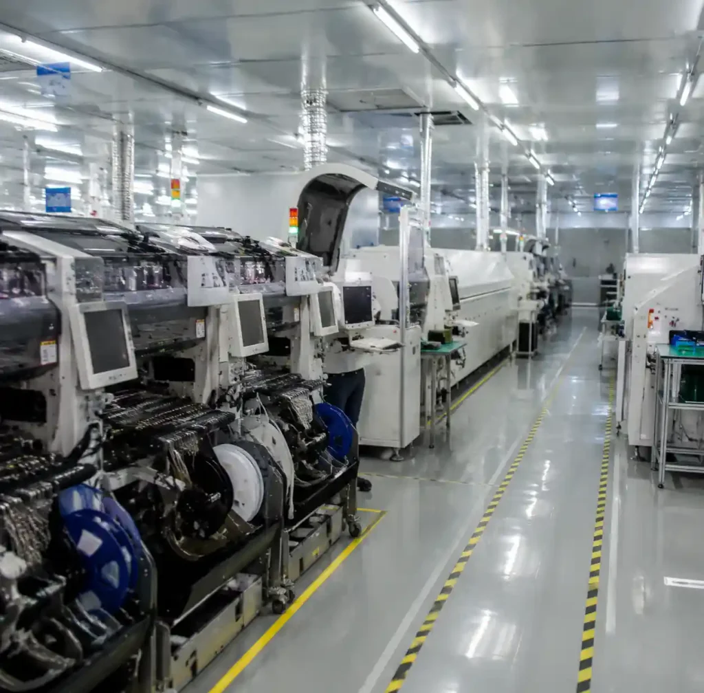
What is PCB Assembly?
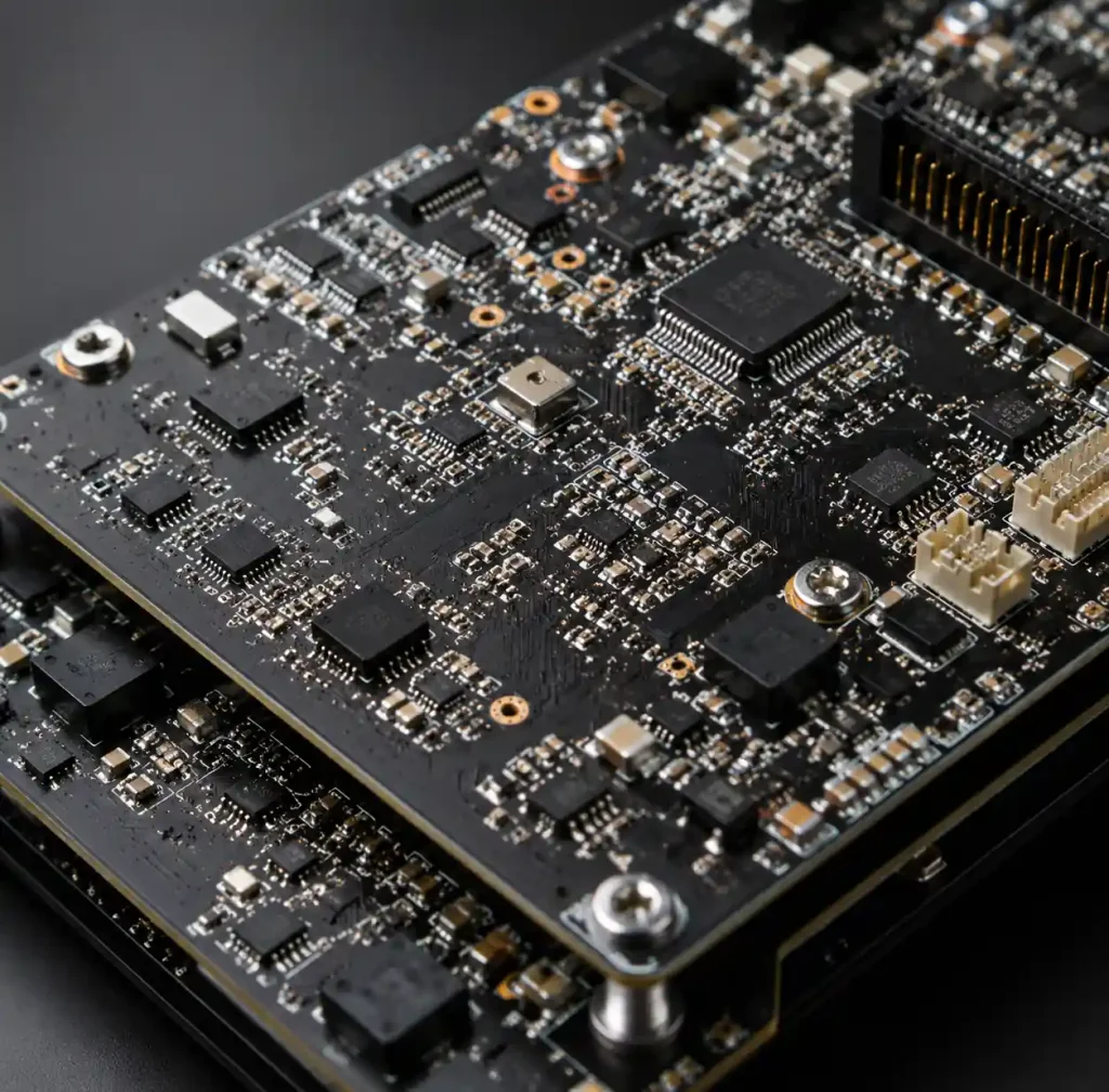
PCB assembly (PCBA) transforms bare circuit boards into functional electronics by attaching components through controlled soldering. The process integrates surface mount technology (SMT), through-hole insertion, and multi-stage inspection.
Modern facilities process mixed-technology boards with components from 01005 resistors (0.4mm × 0.2mm) to large connectors, handling 2-50 layer PCBs. IPC standards mandate 100% inspection for Class 3 assemblies.
Incoming Material Inspection
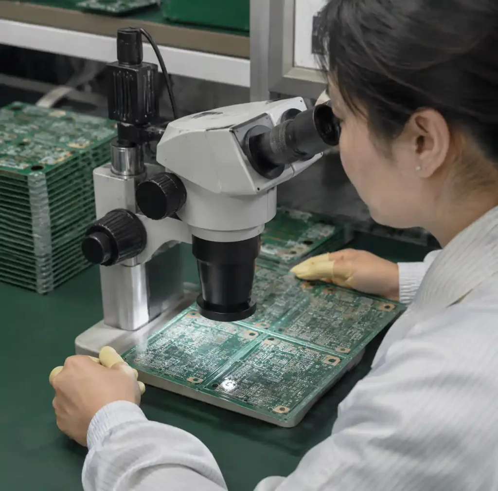
Quality assembly starts with incoming inspection. This checkpoint verifies bare boards and components meet specifications before production begins, catching supplier defects early.
PCB Inspection:
- Visual check for scratches, delamination, warpage, contamination
- Electrical testing for shorts, opens, impedance per IPC-6012
- Dimensional verification using coordinate measuring machines
- Moisture sensitivity level (MSL) rating confirmation
Component Verification:
- Match part numbers against bill of materials (BOM)
- Check packaging integrity and MSL ratings
- Verify date codes and humidity indicators
- Sample testing for electrical parameters
Reject boards with warpage exceeding 0.75% of diagonal length—this causes placement errors during SMT. Components exposed beyond MSL ratings need baking at 40°C for 24-48 hours.
Solder Paste Printing
Solder paste printing deposits precise solder and flux onto PCB pads. Print quality determines 60-70% of final assembly defects—the most critical control point.
Process Parameters:
- Stencil thickness: 0.1-0.15mm for standard SMT, 0.08mm for fine-pitch
- Print speed: 30-80mm/second based on paste rheology
- Squeegee pressure: 0.2-0.4 kg/cm for complete paste release
- Separation speed: 0.5-2mm/second to prevent bridging
Laser-cut stainless steel stencils achieve ±25μm deposit accuracy. Type 3-4 solder paste (25-38μm powder) works for 0.4mm pitch components; Type 5 handles ultra-fine pitch below 0.3mm.
Solder Paste Inspection (SPI):
Inline SPI systems measure paste volume, height, and XY position using laser scanning. Target 100-150μm height with ±25% volume tolerance.
SMT Component Placement
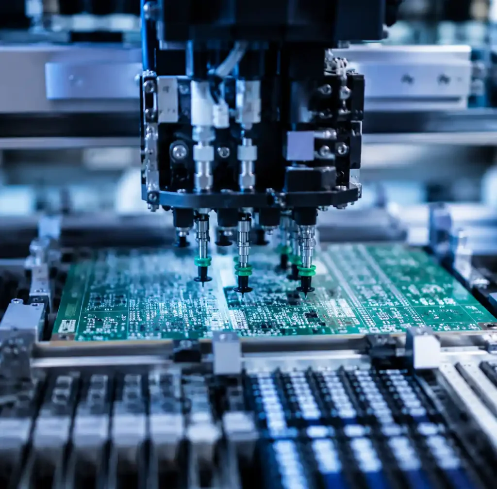
Pick-and-place machines position surface mount components on wet solder paste with ±25-50μm accuracy. High-speed machines place 80,000-100,000 components per hour for passives, while high-accuracy systems handle 0.3mm pitch BGAs and 01005 components.
Placement Sequence:
- Small passives (resistors, capacitors) via high-speed heads
- Active components (ICs, transistors) with vision alignment
- Fine-pitch devices (QFPs, BGAs) via precision systems
- Odd-form components requiring specialized handling
Machine vision uses fiducial marks and component body recognition to correct positioning errors. Proper nozzle selection achieves ±30μm accuracy for 0.4mm pitch devices.
Solder paste has 30-60 minute working time at room temperature before solvent evaporation degrades solderability. Advanced facilities use nitrogen cabinets extending working time to 4-8 hours.
Reflow Soldering Process
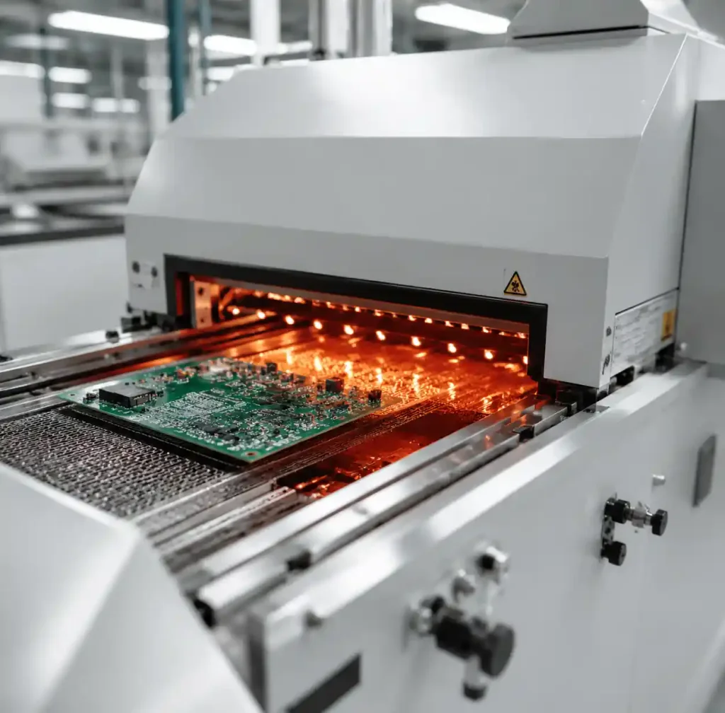
Reflow ovens melt solder paste through controlled thermal profiles, creating metallurgical bonds between components and PCB pads. Lead-free SAC305 solder requires peak temperatures of 240-250°C.
| Reflow Zone | Temperature Range | Duration | Purpose |
|---|---|---|---|
| Preheat | 150-180°C | 60-90s | Activate flux, evaporate solvents |
| Soak | 180-200°C | 60-120s | Equalize thermal mass, reduce delta-T |
| Reflow | 240-250°C peak | 60-90s TAL | Melt solder, form intermetallic bonds |
| Cooling | 6°C/second max | 90-120s | Solidify joints, control grain structure |
Profile each board design using thermocouples at thermal mass points. Heating rate below 3°C/second prevents component cracking; cooling under 4°C/second produces fine-grain structure.
Nitrogen reflow atmosphere (< 500ppm oxygen) improves wetting on difficult surfaces. Standard air reflow works for most assemblies using OSP or ENIG finishes.
Automated Optical Inspection (AOI)
Post-reflow AOI uses high-resolution cameras and algorithms to detect visible defects. 2026 quality standards show AOI catches 85-95% of surface defects.
Detectable Defects:
- Missing or wrong components
- Component polarity and orientation errors
- Solder bridges between adjacent pads
- Insufficient solder on terminations
- Component misalignment exceeding ±50% of pad width
- Solder balls and flux residue
AOI cannot inspect hidden joints under BGA packages or QFN thermal pads. These require X-ray inspection.
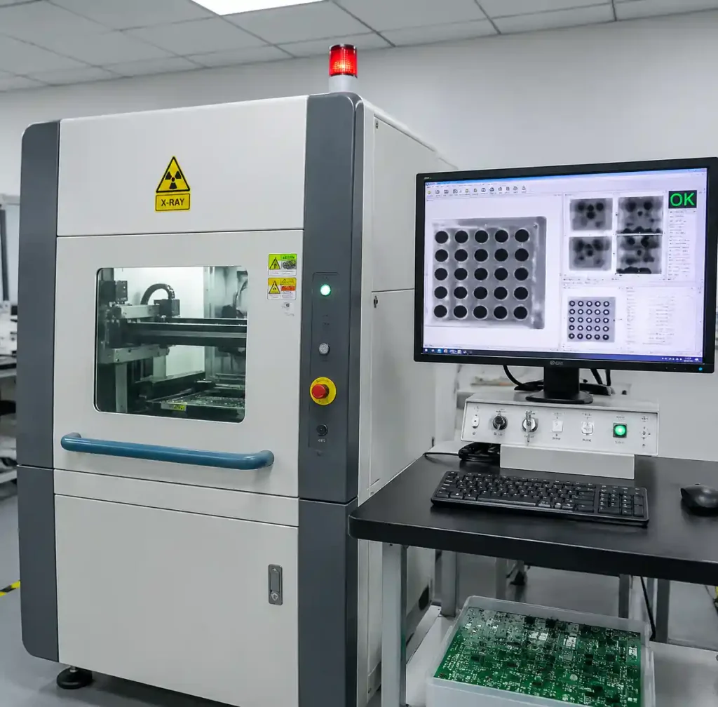
X-Ray Inspection for Hidden Joints
Automated X-ray inspection (AXI) penetrates component bodies to reveal internal solder quality. This non-destructive method is essential for BGA, CSP, and QFN packages.
X-Ray Capabilities:
- Void detection in BGA balls (IPC-A-610 allows 25% void area for Class 2)
- Hidden bridges between BGA balls
- Insufficient solder or non-wetting conditions
- Component co-planarity issues
- Through-hole fill percentage verification
3D X-ray systems use computed tomography for cross-sectional images. Specify X-ray inspection for all BGA assemblies, especially packages with >0.8mm ball pitch.
| Inspection Method | Detects Surface Defects | Detects Hidden Defects | Throughput | Cost |
|---|---|---|---|---|
| Visual | Limited | No | High | Low |
| AOI | Yes | No | High | Medium |
| X-Ray | Limited | Yes | Medium | High |
| ICT | No | Electrical only | Low | High |
| Flying Probe | No | Electrical only | Very Low | Medium |
Through-Hole Component Assembly
After SMT reflow, through-hole components (connectors, transformers, large capacitors) are inserted manually or via automatic insertion machines. Through-hole technology provides mechanical strength for connectors and large components.
Wave Soldering:
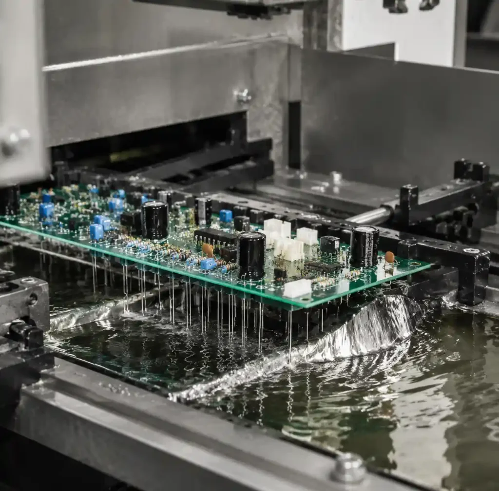
Wave soldering passes boards over molten solder at 250-260°C for lead-free alloys. The 3-5 second contact time works for boards with through-hole components on one side. Proper preheat (90-110°C top-side temperature) achieves consistent hole fill.
Selective Soldering:
Selective soldering uses programmable nozzles to solder individual through-hole locations without exposing the entire board to high temperatures. This protects temperature-sensitive SMT components. Cycle time is 2-5 seconds per joint with nitrogen atmosphere.
Assembly Cleaning
Post-soldering cleaning removes flux residues causing ionic contamination and corrosion. No-clean flux dominates commercial assembly, but high-reliability products require water-based or solvent cleaning.
Cleaning Methods:
- Inline aqueous cleaning with deionized water
- Batch solvent cleaning using modified alcohols
- Ultrasonic cleaning for dense assemblies
Verify cleanliness using ionic contamination testing per IPC-TM-650 or visual inspection under magnification.
Conformal Coating Application
Conformal coating applies a thin protective polymer film over assembled boards to protect against moisture, chemicals, and environmental contamination.
Coating Types:
- Acrylic (AR): Easy rework, good moisture resistance
- Silicone (SR): Wide temperature range, flexible, used in automotive
- Urethane (UR): Superior chemical resistance, difficult to rework
- Parylene (XY): Vacuum-deposited, pinhole-free, biocompatible
Application methods include selective spray, dip coating, and brush application. Masking protects connectors, test points, and areas requiring electrical contact.
Functional Testing
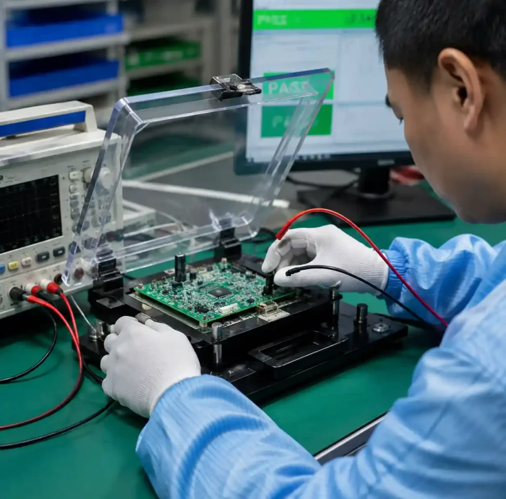
Functional testing verifies assembled boards perform their intended electronic functions. This final quality gate catches defects that passed visual and electrical inspection.
Test Types:
- In-Circuit Testing (ICT): Bed-of-nails fixture tests component values and shorts/opens
- Flying Probe: Programmable probes test boards without custom fixtures
- Functional Test: Power up board and verify all features work per specification
- Burn-in: Extended operation at elevated temperature for 24-168 hours
Test coverage depends on reliability requirements and production volume.
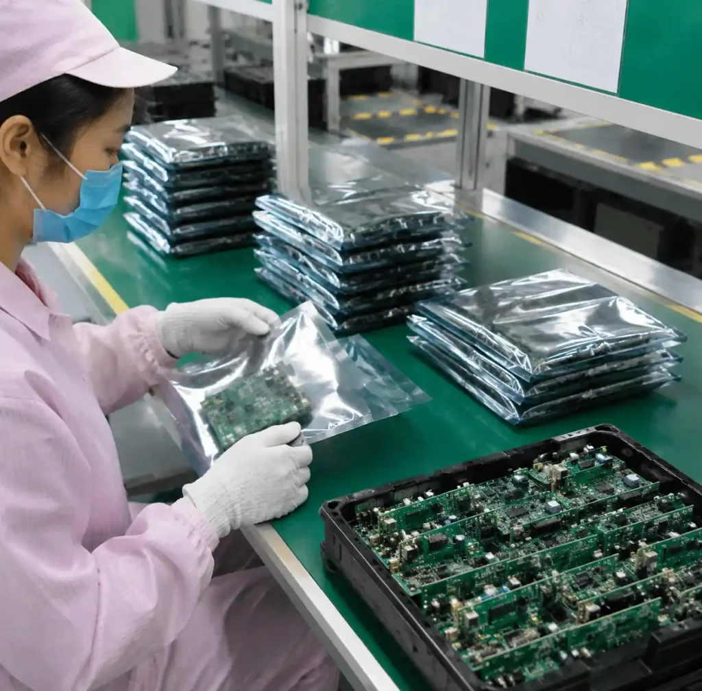
Final Quality Control and Packaging
Before shipment, assemblies undergo final visual inspection and packaging. Quality documentation includes:
- Certificate of conformance
- First article inspection reports
- Traceability records (lot codes, date codes, serial numbers)
- Test data and yield reports
- RoHS/REACH compliance declarations
ESD-safe packaging using moisture barrier bags and desiccants protects assemblies during shipping.
PCB Assembly Process Comparison
| Assembly Type | Component Types | Lead Time | Applications | Relative Cost |
|---|---|---|---|---|
| SMT Only | Surface mount | 3-5 days | Smartphones, tablets, IoT devices | 1.0x |
| Through-Hole Only | Radial/axial leads | 5-7 days | Power supplies, legacy products | 1.2x |
| Mixed Technology | SMT + through-hole | 7-10 days | Industrial controls, automotive | 1.5x |
| Box Build | Full product assembly | 10-15 days | Medical devices, test equipment | 2.0-3.0x |
Andwin Circuits Assembly Capabilities
Andwin Circuits provides turnkey PCB assembly services with advanced SMT and through-hole capabilities for electronics manufacturers worldwide. Our facility handles complex assemblies with fast 7-day turnaround.
Technical Specifications:
- SMT component size: 01005 to large BGAs
- Fine-pitch capability: 0.3mm pitch QFP/BGA
- Through-hole assembly and wave/selective soldering
- X-ray inspection for BGA verification
- Conformal coating application
- Functional testing and burn-in services
Our ISO 9001, IATF 16949, and UL certified facility serves automotive, medical, telecommunications, and industrial markets with IPC-A-610 Class 2/3 standards. We process PCBs from 2 to 50 layers.
FAQ
What is the typical lead time for PCB assembly?
Standard PCB assembly lead time is 7-10 days for mixed-technology boards including SMT and through-hole components. Quick-turn assembly services can deliver prototype quantities in 3-5 days. Production volumes require 2-3 weeks depending on component availability.
How do I choose between SMT and through-hole assembly?
SMT provides higher component density, automated placement, and lower cost. Through-hole assembly offers superior mechanical strength for connectors and large components. Most designs use mixed-technology assembly.
What inspection methods are required for BGA assemblies?
BGA assemblies require X-ray inspection because solder joints hide under the component body. You should specify 2D or 3D X-ray inspection with void analysis per IPC-A-610 criteria.
When is conformal coating necessary?
Conformal coating protects assemblies in humid, chemically aggressive, or contaminated environments. You need coating for outdoor electronics, automotive, industrial controls, and marine equipment.
What PCB surface finish works best for assembly?
ENIG provides excellent solderability and extended shelf life for complex assemblies. HASL offers lower cost for simple products. OSP suits high-volume consumer electronics. Your choice depends on assembly complexity as detailed in our surface finish comparison guide.
Conclusion
Understanding PCB assembly process flow helps hardware engineers optimize product quality and reduce manufacturing costs. Each process step from solder paste printing through final inspection contributes to assembly reliability.
Modern PCBA facilities integrate automated inspection at multiple checkpoints to catch defects early. Proper process control at critical steps—paste printing, component placement, reflow profiling, and X-ray inspection—determines assembly yield.
If you need high-quality PCB assembly for your electronic products, Andwin Circuits offers advanced manufacturing capabilities up to 50 layers with fast turnaround in 7 days. Our ISO 9001, IATF 16949, and UL certified facility serves automotive, medical, telecommunications, and industrial applications worldwide.
Contact us today for custom PCB assembly solutions and competitive pricing.