
PCB Stack-up Calculator: How to Design Optimal Layer Configuration
PCB design complexity increases with layer count, yet 60% of signal integrity failures trace back to improper stackup planning. For engineers designing high-speed circuits above 500 MHz, controlled impedance routing without accurate stackup calculation leads to reflections, crosstalk, and EMI violations that delay product launches by months.
If you want to design optimal PCB stackups, you need to understand layer arrangement principles, dielectric selection, impedance calculation methodology, and online stackup calculator usage. This guide provides actionable strategies based on IPC-2141 impedance standards and manufacturing constraints.
What Is a PCB Stackup Calculator?
A PCB stackup calculator computes electrical and physical properties of multilayer boards based on layer arrangement, material selection, and copper weights. According to IPC-2141A standards, these calculators determine controlled impedance, total thickness, and signal propagation delays by analyzing geometric relationships between copper traces and reference planes through dielectrics.
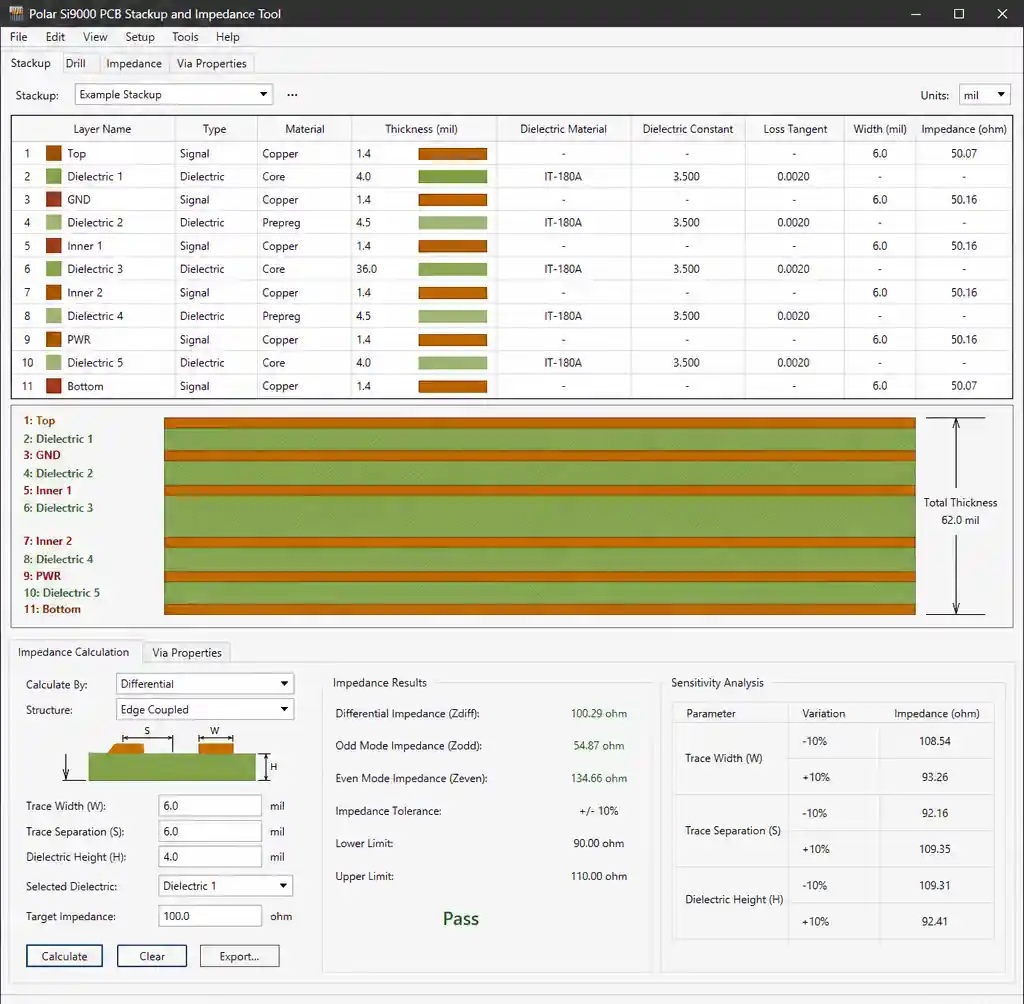
The calculator accepts inputs including trace width, dielectric thickness, copper weight, and dielectric constant (Er) to output characteristic impedance for microstrip and stripline. You should use stackup calculators during early design—before layout begins—to establish manufacturable layer arrangements meeting electrical performance and fabrication capabilities.
Impedance Calculation Fundamentals
Controlled impedance calculation relies on transmission line theory where trace geometry and dielectric properties determine characteristic impedance Z0. For microstrip traces (surface layer with one reference plane), impedance depends on trace width (W), dielectric height (H), copper thickness (T), and material Er per IPC-2141A formulas.
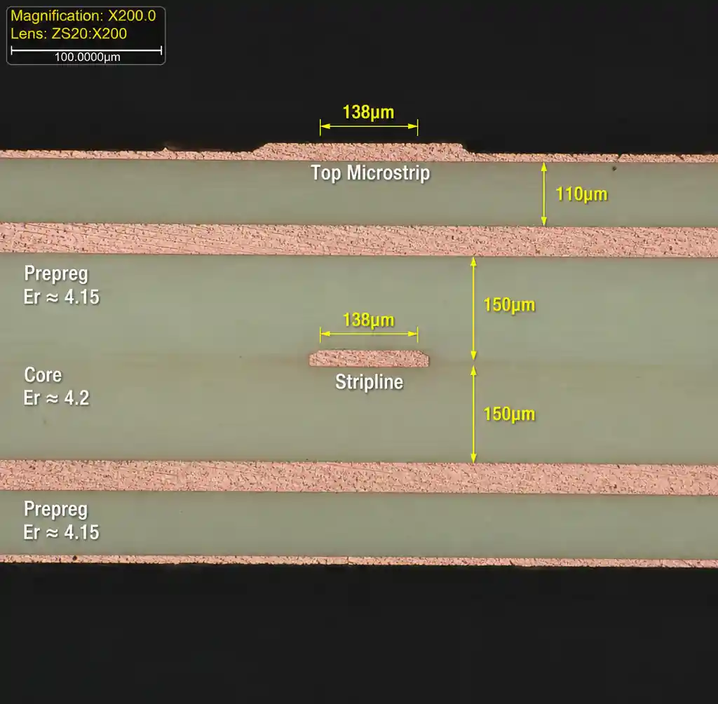
Stripline traces (buried between two reference planes) exhibit lower impedance for equivalent geometries because fields couple to both planes. Target impedance values follow industry conventions: 50Ω single-ended for digital signals, 90Ω differential for USB 2.0, 100Ω differential for PCIe and Ethernet, and 75Ω for video. Manufacturing tolerance typically achieves ±10% (±5Ω for 50Ω traces) with controlled processes.
| Signal Type | Impedance (Ω) | Topology | Tolerance |
|---|---|---|---|
| Digital single-ended | 50 | Microstrip / Stripline | ±10% |
| USB differential | 90 | Differential pair | ±10% |
| PCIe / Ethernet | 100 | Differential pair | ±10% |
| HDMI / DisplayPort | 100 differential | Differential pair | ±10% |
Dielectric Material Selection Criteria
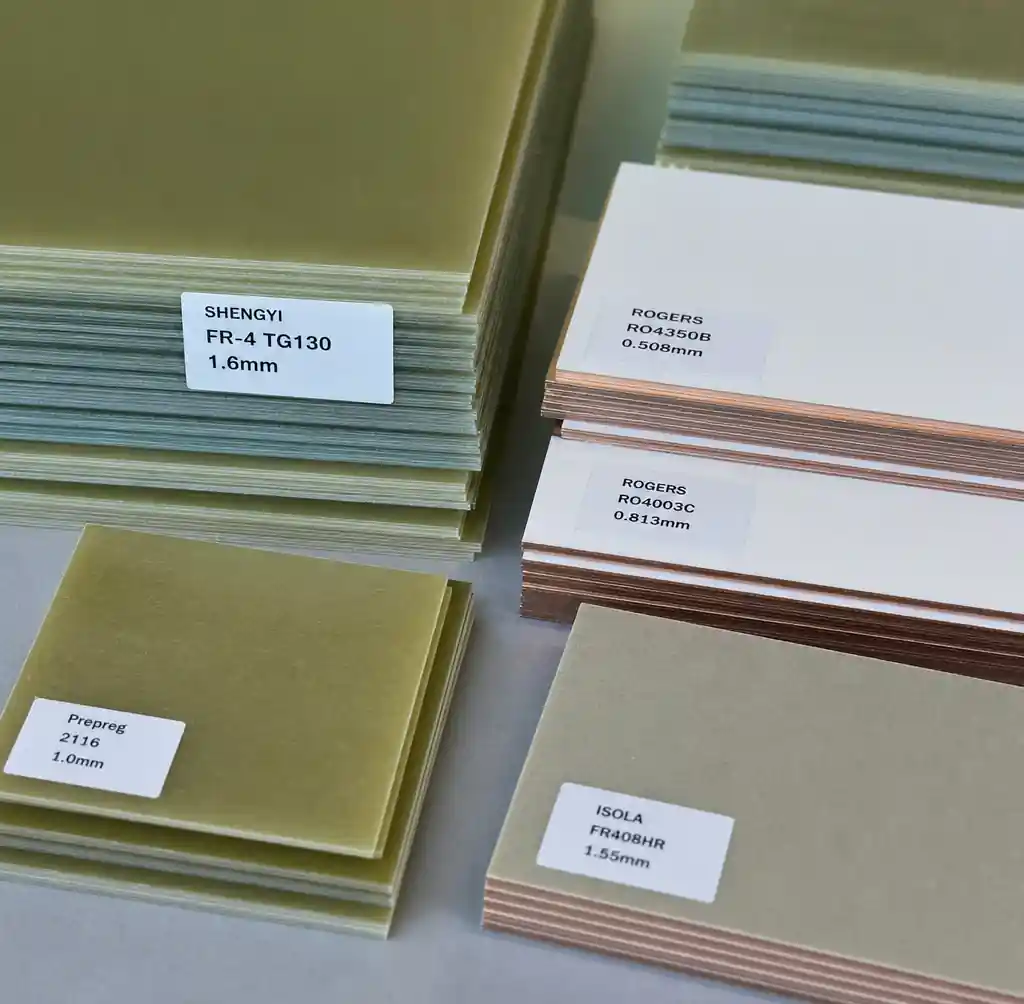
FR-4 standard materials provide Er values from 4.2 to 4.6 at 1 MHz, with variation increasing at higher frequencies. High-frequency laminates like Rogers RO4350B maintain stable Er of 3.48 ±0.05 across 2-10 GHz, critical for RF applications where phase matching determines antenna array performance.
Dielectric loss tangent (tan δ) quantifies signal attenuation. Standard FR-4 exhibits tan δ of 0.02, while low-loss materials achieve 0.002-0.005. For signals above 10 Gbps, dielectric loss dominates insertion loss budget. Thickness tolerance in prepreg affects impedance accuracy—cores maintain ±0.05mm while prepreg varies ±15-20%. Always verify final stackup with your manufacturer’s actual capabilities.
Power and Ground Plane Placement Strategy
Reference plane continuity determines return path quality for high-speed signals. Every signal layer requires an adjacent reference plane (power or ground) within 4-6 mils (0.1-0.15mm) to provide low-inductance return paths. Splitting reference planes creates discontinuities generating EMI above 1 GHz.
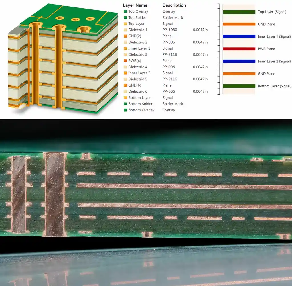
Four-layer stackups arrange as Signal-Ground-Power-Signal, providing solid reference for top and bottom signals. Six-layer boards improve performance with Signal-Ground-Signal-Signal-Ground-Signal, allowing dual stripline routing with excellent EMI shielding. Closely spaced power-ground pairs create distributed capacitance (1000-2000 pF/in²) that lowers PDN impedance across 1-100 MHz, reducing decoupling capacitor count.
Symmetry and Layer Balance Requirements
Balanced copper distribution prevents board warpage during reflow. Asymmetric stackups create thermal expansion mismatch that bows boards by 5-15mm across 300mm panels. IPC-2221B recommends mirroring copper weight and layer structure around centerline.
For 8-layer designs, symmetry appears as L1-L2-L3-L4 mirroring L8-L7-L6-L5, with equal prepreg thickness and copper weight at corresponding positions. High layer count boards (16-24 layers) require sequential lamination in symmetric sub-stacks. Work with manufacturers offering high layer count PCB to optimize lamination sequences minimizing warpage.
| Layer Count | Recommended Stackup | Applications | Thickness (mm) |
|---|---|---|---|
| 4-layer | Sig-Gnd-Pwr-Sig | Consumer electronics, IoT | 1.6 |
| 6-layer | Sig-Gnd-Sig-Sig-Gnd-Sig | USB 3.0, high-speed digital | 1.6 |
| 8-layer | Sig-Gnd-Sig-Pwr-Pwr-Sig-Gnd-Sig | PCIe, DDR4, Ethernet | 1.6-2.0 |
| 10+ layer | Mixed signal/power | Servers, telecom | 2.0-2.4 |
Online Stackup Calculator Tools
Nodeloop’s Calculator provides interactive visualization with layer reordering and real-time impedance calculation for microstrip, stripline, and differential pairs. The tool includes presets for 2/4/6-layer configurations.
FlexiPCB’s Builder focuses on flex and rigid-flex constructions, accounting for coverlay, adhesive layers, and stiffener placement. Professional EDA tools like Altium Designer and Cadence Allegro integrate stackup calculation with layout database, auto-recalculating impedance with design changes.

Stackup Design Process Steps
Start by defining electrical requirements: target impedances (50Ω, 100Ω), frequency range, and signal types. Determine minimum layer count based on routing density and power distribution. Four layers suffice for designs under 1 GHz, while 6-8 layers support GHz signaling.
Select dielectric materials matching frequency requirements and cost constraints. Standard FR-4 works below 2 GHz, while Rogers or Isola laminates serve 5-10 GHz designs. Input manufacturer’s material specifications (Er, thickness tolerance, copper weight) into the calculator for accurate results.
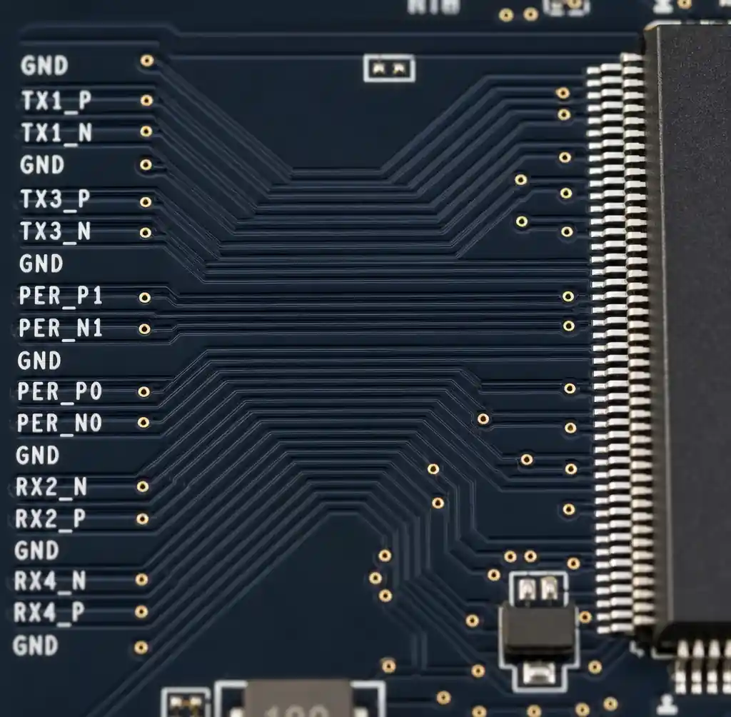
Calculate trace width for target impedance on each layer. Microstrip traces typically require 4-6 mil widths for 50Ω with 4-5 mil dielectric height. Stripline achieves 50Ω with 3-4 mil widths. Verify calculated widths meet manufacturer’s minimum trace/space—typically 3/3 mil for HDI PCB and 5/5 mil for standard PCB. Adjust prepreg thickness to fine-tune impedance if trace width hits process limits.
Copper Weight Impact on Impedance
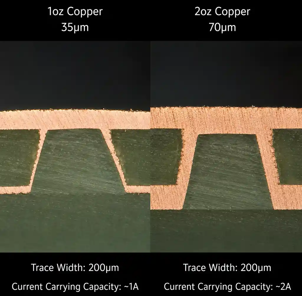
Standard fabrication uses 1oz (35μm) copper. Thicker copper—2oz (70μm) or 3oz (105μm)—serves high-current applications but affects impedance. A 5 mil trace in 1oz copper etches to ~4.5 mil average width, while 2oz produces ~4.0 mil due to deeper etching sidewall taper.
For 50Ω microstrip, increasing from 1oz to 2oz copper requires widening traces by 0.5-1.0 mil to maintain target impedance. High-current power traces use 2oz copper to reduce resistive losses—a 50 mil trace in 1oz carries ~3A with 10°C rise, while 2oz carries ~5A. Work with manufacturers experienced in heavy copper PCB to optimize performance tradeoffs.
Prepreg vs Core Material Selection
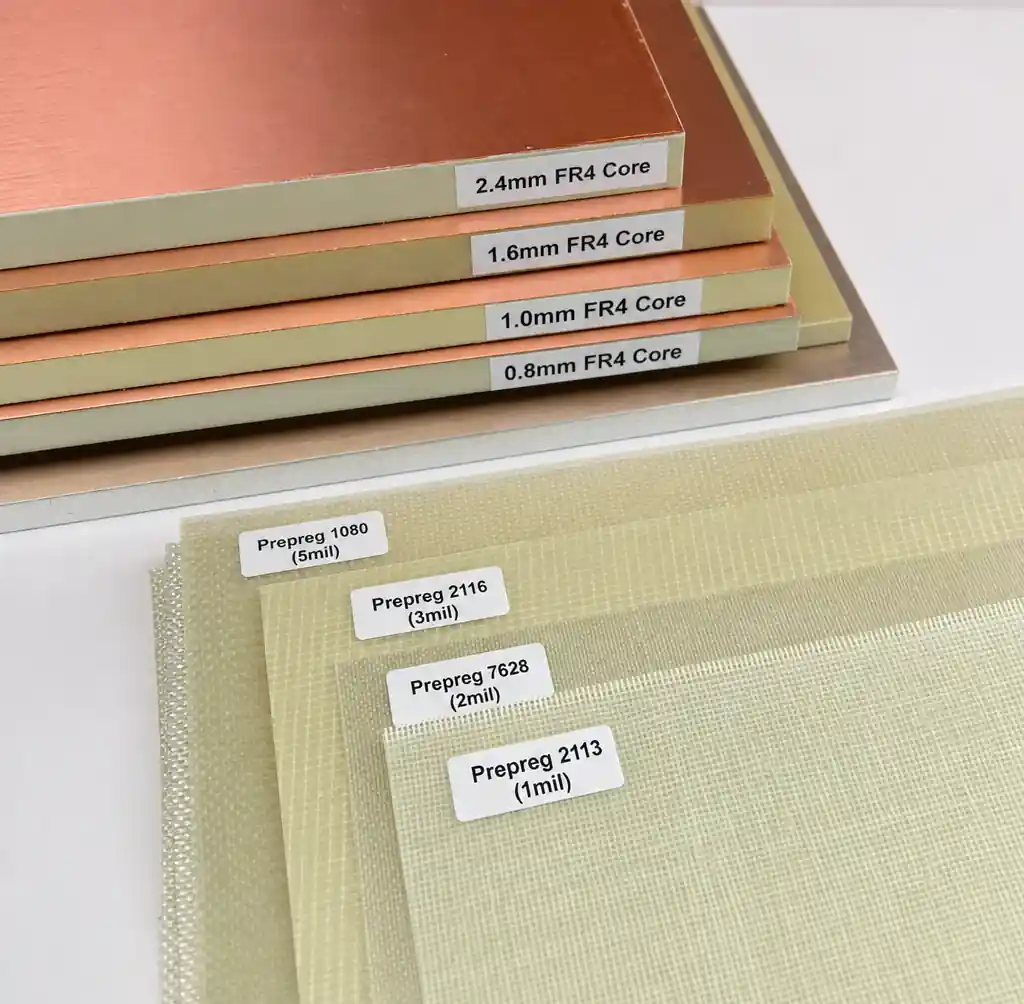
Core materials are rigid copper-clad laminates pre-manufactured in standard thicknesses from 2-60 mil with consistent Er and ±0.05mm tolerance. Prepreg (pre-impregnated) materials consist of glass fabric with partially cured resin that flows during lamination at 170-180°C, bonding cores and copper foils. Final prepreg thickness depends on copper coverage—100% coverage compresses less than 10% coverage, creating ±10-20% variation.
For critical impedance layers, position traces adjacent to core dielectric where thickness remains stable. Place less critical routing adjacent to prepreg where ±15% variation has acceptable impact. Four-layer boards use one core (layers 2-3) with prepreg bonding outer foils. Six-layer constructions use two cores with three prepreg layers.
Specify thin cores (4-6 mil) between differential pairs or power-ground planes to achieve target impedance. Balance core placement symmetrically around stackup centerline to prevent warpage. High-speed designs above 10 Gbps should specify spread glass or low-weave prepreg minimizing Er variation. Discuss material availability during early-stage DFM review.
Manufacturing Verification and Testing
After calculating optimal stackup, encode impedance-controlled net classes in PCB design tools with calculated trace widths. Altium, Cadence, and KiCAD support design rules specifying width constraints for specific nets, preventing violations during routing.
Document stackup in fabrication drawings including exact material callouts by manufacturer part numbers (e.g., Shengyi S1000-2M, Isola FR408HR). Include total finished thickness, copper weight per layer, and impedance requirements with test coupon specifications. TDR (Time Domain Reflectometry) testing measures actual impedance of manufactured test coupons replicating critical traces at panel edge.
Manufacturing achieves ±8-10% impedance tolerance under standard controls, tightening to ±5% with enhanced controls. Specify impedance acceptance criteria in fabrication notes—for example, “50Ω ±5Ω measured per IPC-TM-650.” Partner with manufacturers experienced in controlled impedance PCB to establish testing protocols.
FAQ
What is the purpose of a PCB stackup calculator?
A stackup calculator determines physical layer arrangement and electrical properties of multilayer PCBs, calculating controlled impedance, board thickness, and material specifications needed for manufacturing before starting layout.
How do I calculate 50Ω impedance for my PCB?
Input dielectric Er value (typically 4.2-4.4 for FR-4), dielectric thickness (4-6 mils), copper weight (1oz), and desired impedance into a calculator. The tool calculates required trace width, typically 4-6 mils for microstrip and 3-4 mils for stripline.
What is the difference between microstrip and stripline?
Microstrip routes on outer layers with one reference plane below, while stripline routes on inner layers between two reference planes. Stripline provides better EMI shielding and tighter impedance control but requires additional layers.
Should I use core or prepreg for impedance-controlled layers?
Position impedance-critical traces adjacent to core layers where thickness maintains ±0.05mm tolerance. Prepreg varies ±15-20% based on copper coverage, making it less suitable for tight impedance control.
How does copper weight affect stackup impedance?
Heavier copper (2oz vs 1oz) reduces effective trace width after etching, requiring 0.5-1.0 mil additional width to maintain target impedance. Always specify copper weight in calculations for accurate prediction.
Conclusion
Accurate stackup calculation balances electrical performance, mechanical stability, and manufacturing feasibility. By understanding impedance principles, material selection, and layer arrangement strategies, you can design multilayer PCBs meeting signal integrity requirements while remaining cost-competitive. Online calculators streamline this process, allowing rapid iteration before layout commitment.
Andwin Circuits offers advanced manufacturing capabilities up to 50 layers with precise impedance control. Our engineering team provides DFM analysis and stackup optimization ensuring designs meet electrical specifications and manufacturing tolerances. We have delivered impedance-controlled PCBs for telecommunications, automotive, medical, and computing applications worldwide. Contact us for custom stackup design support and fast turnaround in 7 days.