
PCB Design for Explosive Atmospheres: ATEX and IECEx Compliance
Explosive atmosphere equipment failures cause over 200 industrial incidents annually in oil refineries, chemical plants, and mining operations. A single spark from improperly designed electronics in Zone 1 hazardous areas can ignite flammable gases and trigger catastrophic explosions. Equipment certification to ATEX and IECEx standards prevents these disasters.
If you want to design PCBs for hazardous locations, you need to understand zone classification, protection methods, creepage and clearance requirements, encapsulation techniques, and certification processes per IEC 60079 standards. This guide provides practical design rules from oil and gas, petrochemical, and mining industry applications.
What Are ATEX and IECEx Standards?
ATEX is the European Union regulatory directive (2014/34/EU) mandatory for equipment sold in the European Economic Area for use in potentially explosive atmospheres. The directive came into force on April 20, 2016, and covers manufacturers, importers, and distributors of electrical and mechanical equipment. According to ATEX directive regulations, equipment must undergo conformity assessment procedures and carry CE marking with the Ex symbol.
IECEx is an international certification scheme managed by the International Electrotechnical Commission that allows a single test report to be accepted across 39 participating countries. Both ATEX and IECEx align with the same underlying technical standards—the IEC 60079 series—so there is essentially no technical difference between them. The primary distinction is regulatory scope: ATEX is legally required in the EU, while IECEx provides voluntary international recognition accepted in Asia-Pacific, Middle East, and other regions.
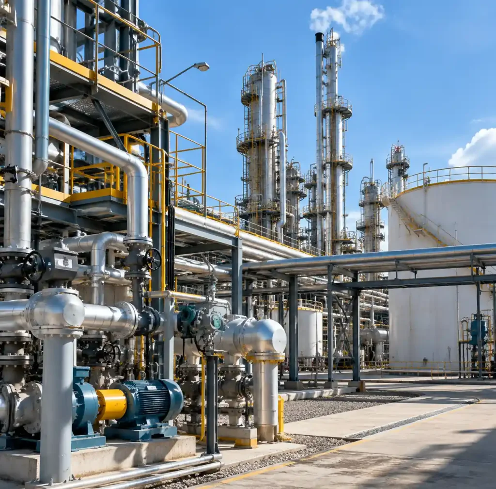
PCBs themselves are not typically certified independently. ATEX and IECEx approvals are evaluated at the complete equipment, assembly, or enclosure level rather than at the bare board stage. However, PCB design directly determines whether the final product can achieve certification. Poor board-level design choices—inadequate spacing, wrong materials, excessive temperatures—cause certification failures after expensive prototyping and testing.
Zone Classification and Equipment Categories
Explosive atmosphere zones classify the likelihood and duration that flammable gases, vapors, or combustible dusts are present. This classification determines the required equipment protection level and acceptable ignition risk.
Gas and vapor zones divide into three categories based on presence duration. Zone 0 indicates explosive atmosphere present continuously or for long periods—typically found inside storage tanks or process vessels. Zone 1 means explosive atmosphere likely to occur occasionally during normal operations, existing 10 to 1000 hours per year. Zone 2 covers areas where explosive atmosphere is unlikely to occur, or only briefly if it does, typically existing less than 10 hours annually. Most PCB applications target Zone 2 or Zone 1 installations.
Equipment categories match to zone requirements with descending protection levels. Category 1G equipment provides very high protection suitable for Zone 0, 1, and 2 locations through two independent protection means or high safety factors. Category 2G offers high protection for Zone 1 and 2 through proven protection concepts. Category 3G provides normal protection adequate for Zone 2 only, designed to prevent ignition during normal operation.
Gas groups further classify ignition sensitivity. Group IIA covers less easily ignitable gases like propane and methane. Group IIB includes intermediate sensitivity gases such as ethylene. Group IIC encompasses the most easily ignitable gases including hydrogen and acetylene. Equipment rated for Group IIC can operate in IIA and IIB environments, but not vice versa. Your PCB design must account for the most sensitive gas group expected.
| Zone | Explosive Atmosphere Duration | Equipment Category | Protection Level |
|---|---|---|---|
| Zone 0 | Continuous or long periods | Category 1G (EPL Ga) | Very High (two independent means) |
| Zone 1 | Occasional during normal operation | Category 2G (EPL Gb) | High (proven protection) |
| Zone 2 | Unlikely or brief | Category 3G (EPL Gc) | Normal (prevent ignition) |
Temperature classification specifies maximum surface temperature of electrical equipment to prevent ignition of surrounding atmosphere. T1 equipment allows 450°C maximum surface temperature, T2 permits 300°C, T3 allows 200°C, T4 restricts to 135°C, T5 limits to 100°C, and T6 requires temperatures below 85°C. PCB thermal design including component power dissipation, copper weight, and thermal management must ensure maximum temperatures stay within the specified T-class under all operating conditions including fault scenarios.
Intrinsic Safety Protection Method
Intrinsic safety (Protection type “i” per IEC 60079-11) limits electrical energy in circuits to levels so low they cannot produce sparks or temperatures sufficient to ignite explosive atmospheres. This protection method is the most common for PCB applications because it allows equipment to remain energized in hazardous areas without explosion-proof enclosures.
The fundamental principle restricts voltage, current, and stored energy below ignition thresholds even under fault conditions. According to intrinsically safe PCB design standards, designers must consider shorts, opens, and ground faults. Maximum voltage is typically limited to 30V, with current restrictions depending on the gas group and fault scenario. Capacitive and inductive energy storage must be calculated and proven safe through worst-case analysis.
Equipment protection levels within intrinsic safety vary. Level “ia” provides very high protection suitable for Zone 0, maintaining safety with two countable faults. Level “ib” offers high protection for Zone 1, maintaining safety with one countable fault. Level “ic” provides enhanced protection for Zone 2, maintaining safety under normal operation and one fault. Most industrial sensor and control applications target “ib” protection.
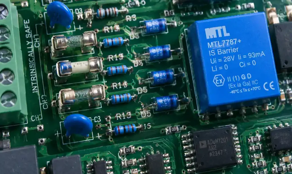
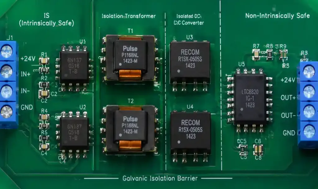
Energy limitation requires careful circuit design. Zener diodes provide voltage clamping, current-limiting resistors restrict fault currents, and galvanic isolation separates intrinsically safe circuits from higher-energy power systems. Stored energy in capacitors and inductors must be calculated using formulas from IEC 60079-11, which account for gas group minimum ignition energy. For Group IIC hydrogen atmospheres, ignition energy is approximately 20 microjoules, requiring extremely small capacitance and inductance values in intrinsically safe circuits.
Creepage and Clearance Requirements
Creepage and clearance distances prevent electrical breakdown and arcing between conductors of different potentials. These spacing requirements are critical for maintaining intrinsic safety and preventing ignition sources on PCBs in hazardous locations.
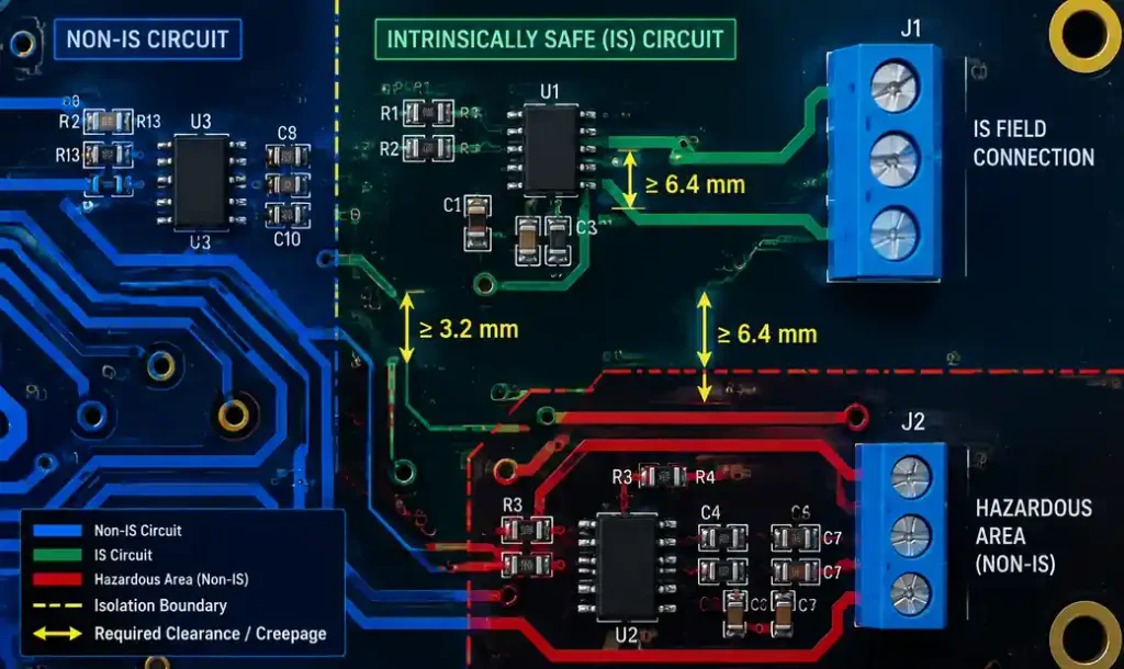
Clearance is the shortest distance through air between two conductive parts. Creepage is the shortest path along the surface of insulation between conductors. IEC 60079-11 specifies minimum values based on voltage difference, pollution degree, and material group. For intrinsically safe circuits operating at 30V, minimum clearance typically ranges from 1.0mm to 3.0mm depending on whether the spacing is within intrinsically safe circuitry or between intrinsically safe and non-intrinsically safe portions.
PCB layout must ensure adequate spacing between traces, component leads, and terminals. Use wider spacing than standard consumer electronics—increase trace-to-trace clearance to minimum 0.5mm for low-voltage intrinsically safe circuits, and 3.0mm or greater when separating intrinsically safe circuits from higher-energy sections. According to IEC 60079-11 requirements, pollution degree 2 (normal industrial environment) is typically assumed unless conformal coating or encapsulation provides pollution protection.
Component selection impacts spacing. Surface-mount components with fine pitch create spacing challenges. Through-hole components generally provide better inherent spacing and mechanical robustness. Optocouplers and isolation transformers used for galvanic isolation must be certified for the required separation voltage and provide adequate creepage distances. Verify optocoupler datasheets specify ATEX or IECEx compliance.
| Circuit Separation | Min Clearance (mm) | Min Creepage (mm) | Typical Application |
|---|---|---|---|
| Within IS circuit (≤30V) | 1.0 | 1.5 | Sensor signal routing |
| IS to non-IS (safe-side) | 3.0 | 6.0 | Barrier interface |
| Non-IS to ground | 0.5 | 1.0 | Power supply common |
| Isolation barrier | 8.0 | 10.0+ | Galvanic isolation |
Encapsulation Protection Method
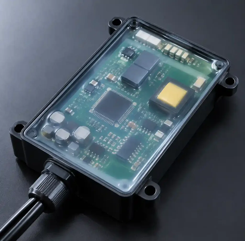
Encapsulation (Protection type “m” per IEC 60079-18) prevents explosive atmospheres from contacting ignition-capable parts on PCBs by embedding electronics in compound that cures to form a protective barrier. This method is particularly effective for complex PCBs where achieving intrinsic safety through energy limitation is impractical due to power requirements or circuit complexity.
Potting compounds used for encapsulation include epoxy resins, polyurethane, and silicone. Epoxy provides maximum mechanical strength and chemical resistance with Shore D hardness 75-90, making it suitable for harsh chemical environments. Polyurethane offers flexibility with Shore A hardness 60-90, absorbing vibration and thermal cycling stress. Silicone provides the widest temperature range (-60°C to +200°C) and lowest modulus, reducing stress on components during thermal expansion.
The encapsulation process involves placing the populated PCB into a mold or potting box and pouring compound to completely cover all components and exposed conductors. Cure time ranges from 2 hours for fast-cure formulations to 24-48 hours for full polymerization. Post-cure heating at 80-100°C for 2-4 hours improves mechanical properties and reduces residual volatiles. The cured encapsulant must be free of voids larger than 1mm³ and provide minimum 3mm thickness over components.
According to IEC 60079-18 encapsulation standards, the compound must maintain integrity over the equipment’s rated temperature range and withstand environmental exposure including chemicals, UV radiation, and humidity. Testing includes thermal cycling, impact resistance, and verification that the encapsulated assembly does not become an ignition source when subjected to maximum operating temperature.
PCB Material Selection and Thermal Management
PCB substrate material affects flammability ratings and thermal performance critical for hazardous location certification. Standard FR-4 with UL 94V-0 flammability rating meets most requirements, though high-temperature applications benefit from polyimide or ceramic substrates with glass transition temperatures (Tg) from 170°C to 250°C.
Copper weight impacts current carrying capacity and thermal dissipation. Specify 2oz (70µm) copper for power traces carrying over 1A current to maintain trace temperature within safe limits. Temperature rise calculations must account for worst-case ambient conditions plus solar heating for outdoor installations. According to PCB material properties, higher Tg materials maintain mechanical strength at elevated temperatures, reducing risk of board warping that could compromise encapsulation integrity.
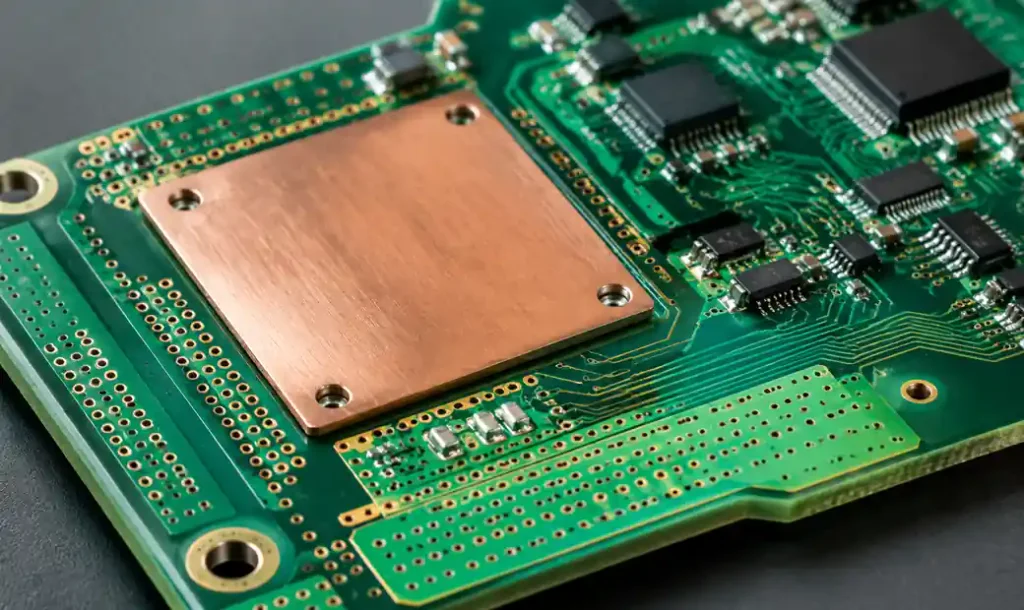
Thermal management becomes critical when maximum surface temperature must remain below T4 (135°C) or stricter classifications. Use thermal vias to conduct heat from high-power components to copper planes or heat sinks. Metal core PCBs with aluminum substrates provide 5-10 times better thermal conductivity than FR-4, making them suitable for LED and power electronics in hazardous locations. Calculate component junction temperatures including thermal resistance from junction to case, case to board, and board to ambient.
Conformal coating provides additional moisture and chemical protection without the complete encapsulation of potting. Acrylic, urethane, silicone, and parylene coatings with 25-125µm thickness protect against humidity and contamination. However, conformal coating alone does not provide ignition protection—you still need intrinsic safety or other approved protection methods. Apply coating in controlled thickness avoiding pooling that creates conductive bridges.
Component Selection and Circuit Design
Component ratings must provide adequate safety margins for fault scenarios. Voltage ratings should be minimum 2× the maximum applied voltage, and power ratings should be 50% derated from datasheet values to account for elevated ambient temperatures in hazardous locations. Semiconductors must withstand reverse voltage and current surges without breakdown.
Safety barriers and zener diodes limit energy entering intrinsically safe circuits. Zener diodes must be rated for continuous operation at the clamping voltage with sufficient power dissipation capability. Use redundant zeners in series or parallel configurations for “ia” protection requiring two independent protective elements. Fuses and current-limiting resistors provide overcurrent protection, with values calculated to ensure safe operation under worst-case fault scenarios.
Galvanic isolation separates intrinsically safe circuits from higher-energy portions of the system. Optocouplers, isolation transformers, and isolated DC-DC converters must meet the required isolation voltage—typically 500V minimum, 1500V for industrial applications. Verify that isolation components are certified for pollution degree 2 and maintain required creepage distances. Capacitive coupling across the isolation barrier must remain below the safe capacitance limits specified in IEC 60079-11.
Avoid microcontrollers and digital circuits with rapid switching that generate electromagnetic interference. Fast clock edges produce RF emissions that can couple into intrinsically safe circuits, potentially increasing energy beyond safe limits. Use slower clock speeds where possible, and implement proper EMI filtering with ferrite beads and capacitors positioned outside the intrinsically safe zone.
Certification Process and Testing Requirements
The certification process begins with selecting a notified body (for ATEX) or certification body (for IECEx) experienced in your equipment type. Notified bodies are designated organizations authorized to perform conformity assessment—over 30 exist for ATEX, including TÜV, UL, Intertek, and DNV. Certification costs typically range from $15,000 to $50,000 depending on protection type complexity and testing requirements.
Technical documentation includes design drawings showing circuit schematics, PCB layouts with spacing annotations, bill of materials with component datasheets, and safety calculations proving intrinsic safety or other protection effectiveness. Risk assessment documentation per ISO 31000 identifies potential ignition sources and demonstrates that each has been eliminated or controlled. Manufacturing quality procedures per ISO 9001 ensure consistent production.
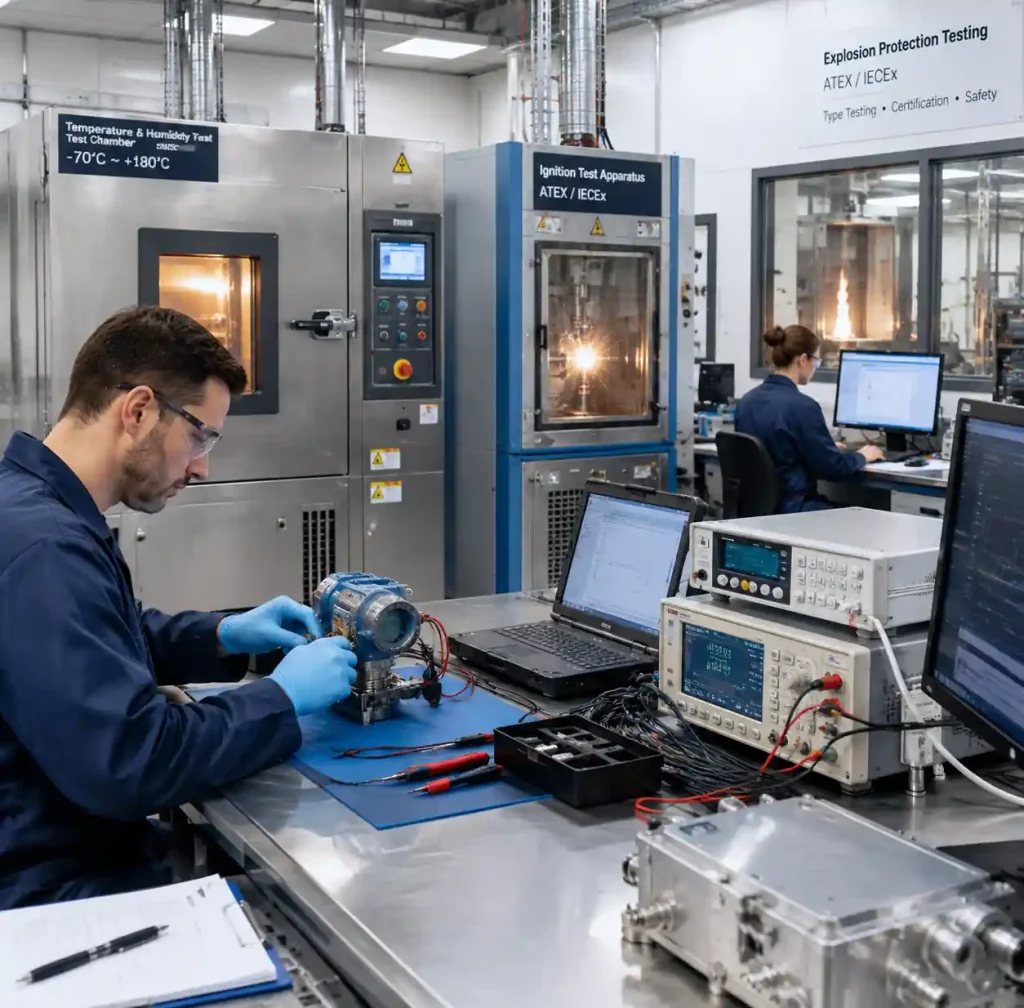
Type testing validates the design under worst-case conditions. Tests include temperature measurements at maximum ambient and overload, short-circuit and open-circuit fault simulations, impact and drop tests per IEC 60068-2-27, and thermal cycling from minimum to maximum rated temperatures. For encapsulated equipment, specimens undergo thermal shock, mechanical shock, and dissection to verify compound coverage and void content.
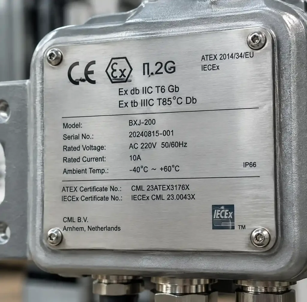
Marking requirements for ATEX include the CE symbol, notified body identification number, Ex symbol, equipment group and category (e.g., II 2G), protection type (e.g., Ex ib IIC T4), and optional ambient temperature range. IECEx marking specifies Ex symbol, certificate number, equipment protection level (e.g., Gb), protection type, gas group, and temperature class. Markings must be permanent and remain legible throughout equipment service life.
Design Guidelines and Common Pitfalls
Inadequate spacing between conductive parts is the most frequently identified problem during design reviews. According to common intrinsically safe design mistakes, designers often apply standard consumer electronics spacing rules rather than the stricter requirements for hazardous locations. Verify that all trace-to-trace, trace-to-plane, and component-to-component spacing meets or exceeds IEC 60079-11 tables.
Energy storage components require careful calculation. Capacitors and inductors in intrinsically safe circuits must remain below safe values that depend on gas group and circuit voltage. For Group IIC hydrogen applications, total circuit capacitance often cannot exceed 1-5µF, and inductance must stay below 1-10mH. These limits severely constrain filter design and require low-ESR ceramic capacitors rather than larger electrolytic types.
Temperature classification violations occur when junction temperatures of semiconductors exceed safe limits. Power MOSFETs, voltage regulators, and high-brightness LEDs generate significant heat. Thermal simulations using finite element analysis should verify that maximum surface temperatures remain at least 20°C below the T-class limit, providing safety margin for ambient temperature variations and component aging. Consider thermal via design to improve heat transfer.
Documentation errors cause certification delays. Schematics must show intrinsically safe portions clearly separated from non-intrinsically safe circuits using dashed lines or different colors. All protection components—zener diodes, fuses, resistors—must be annotated with ratings and part numbers traceable to approved component lists. Assembly drawings must specify conformal coating or potting requirements with material specifications and application procedures.
Frequently Asked Questions
What is the difference between ATEX and IECEx certification?
ATEX is the mandatory European regulatory framework per Directive 2014/34/EU for equipment in the European Economic Area. IECEx is an international voluntary certification accepted in 39 countries including Australia, India, and many Asian nations. Both use identical technical standards (IEC 60079 series), so design requirements are the same. Equipment can obtain both certifications using the same test reports.
Do PCBs require separate ATEX certification?
No. PCBs are components within complete equipment assemblies. ATEX and IECEx certification applies to the finished product—the sensor, controller, or device containing the PCB. However, the PCB design directly determines whether the product can achieve certification. Non-compliant board spacing, materials, or thermal design causes certification failures.
What are typical certification costs and timelines?
Certification costs range from $15,000 to $50,000 depending on protection method complexity, number of equipment variations, and testing scope. Timeline spans 3-6 months including design review, sample submission, type testing, and certificate issuance. Rush services reduce timelines to 6-8 weeks with premium fees. Budget additional costs for design revisions if initial submission fails testing.
Can you retrofit existing PCBs for hazardous location use?
Retrofitting is difficult because fundamental design requirements like spacing, energy limitation, and materials must be designed in from the start. Surface modifications like conformal coating or selective potting may allow marginal improvements, but achieving full compliance usually requires board redesign. If the product requires certification for market access, plan for hazardous location requirements during initial PCB design rather than attempting post-design adaptation.
Which protection method should you choose for your application?
Intrinsic safety (“i” protection) works best for low-power sensors, transmitters, and control circuits under 1W power consumption. Encapsulation (“m” protection) suits higher-power applications where energy limitation is impractical. Explosion-proof enclosures work for high-power equipment like motors and heaters. For PCB assembly applications, intrinsic safety offers the most cost-effective solution when energy requirements permit.
What testing is required during certification?
Type testing includes electrical safety verification with short-circuit and open-circuit fault injection, thermal testing measuring temperatures under maximum load and ambient conditions, mechanical tests including impact and vibration per IEC 60068, and environmental testing with humidity, corrosion, and thermal cycling. Encapsulated assemblies undergo dissection to verify compound coverage. Testing typically requires 6-12 samples.
Conclusion
PCB design for explosive atmospheres requires systematic attention to zone classification, protection methods, spacing requirements, thermal management, and certification testing per IEC 60079 standards. ATEX and IECEx compliance depends on integrating these requirements from initial design rather than attempting retrofit after prototyping. Intrinsic safety provides the most practical protection method for sensor and control electronics, while encapsulation suits higher-power applications.
Andwin Circuits manufactures PCBs for hazardous location applications with design verification for creepage and clearance requirements, high-Tg materials for thermal stability, and multilayer stackup configurations supporting isolation barriers. Our engineering team provides design review for ATEX and IECEx compliance before prototype PCB fabrication. With ISO 9001 certified manufacturing and IPC-6012 Class 3 quality standards, we support oil and gas, chemical processing, and mining industry applications requiring explosion-protected electronics.
Contact us today for PCB manufacturing services supporting hazardous location certification with fast delivery and competitive factory-direct pricing.