
PCB Wave Soldering: Design Rules for Through-Hole Assembly
Wave soldering remains the backbone of high-volume through-hole assembly, but design mistakes cost you time, money, and reliability. After 15 years optimizing production lines at Andwin Circuits, I’ve seen every failure mode—from bridging disasters to cold joints that escape inspection. This guide shares the design rules that separate efficient assembly from expensive rework.
Understanding Wave Soldering Fundamentals
Wave soldering passes your PCB over a turbulent wave of molten solder at 250-260°C. The solder wets exposed copper, wicks up component leads, and forms joints as the board exits. Unlike selective soldering or hand assembly, wave soldering touches everything on the bottom side simultaneously—which means your design must account for every interaction.
The process exposes three critical failure points: inadequate heat transfer to heavy copper areas, solder shadowing where tall components block shorter ones, and bridging between closely-spaced pads. Each requires specific design countermeasures.
Component Orientation and Placement Strategy
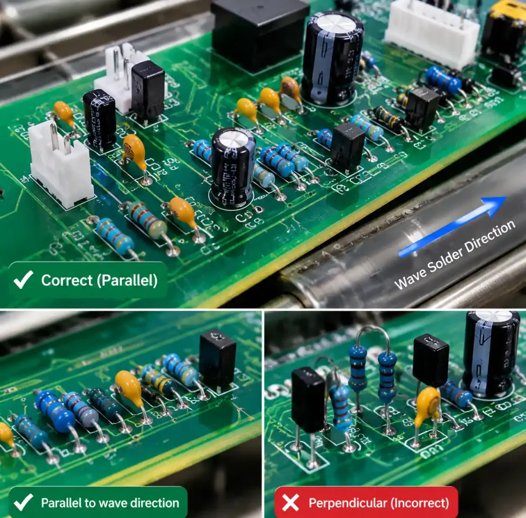
Your component orientation determines whether solder flows cleanly or creates defects. Orient all through-hole components with their long axis parallel to the solder wave direction. This isn’t aesthetic preference—it’s physics. When leads run perpendicular to wave travel, the trailing edge creates turbulence that traps air and causes voids.
Place taller components downstream from shorter ones. A 15mm electrolytic capacitor positioned before a 5mm resistor creates a solder shadow that starves the resistor of wetting. We’ve measured shadow zones extending 8-12mm behind tall components at typical conveyor speeds of 1.2m/min.
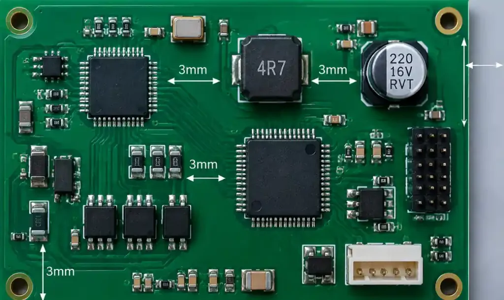
Maintain 3mm minimum spacing between adjacent through-hole components. Industry guidance suggests 1.27mm (50 mils), but production reality demands more margin. Components closer than 3mm experience bridging rates above 2% even with optimized parameters—unacceptable for any serious production environment.
Pad and Hole Design Requirements
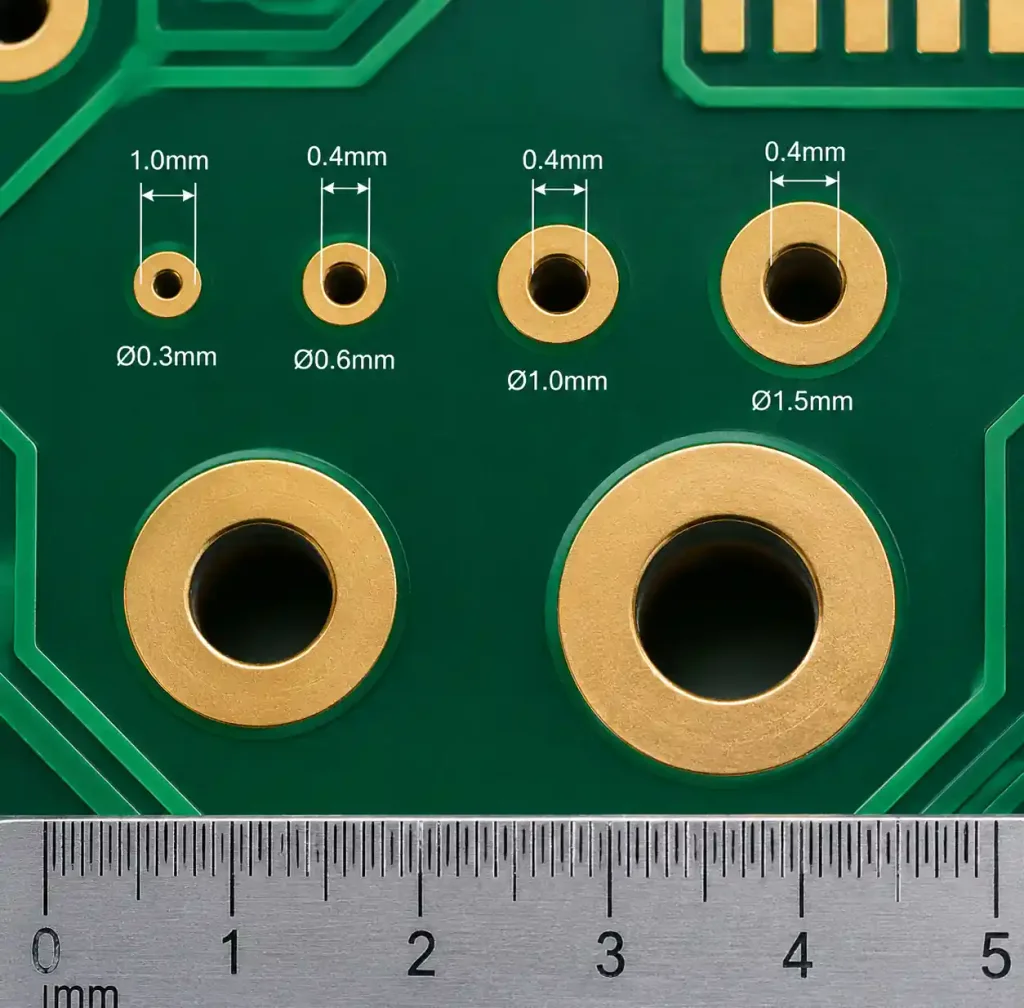
Your pad geometry directly impacts solder joint quality. Design annular rings with 0.4mm minimum width on all layers. Smaller rings risk breakout during drilling tolerance stack-up, leaving insufficient copper for reliable mechanical attachment. For high-reliability applications, increase this to 0.5mm.
Hole size selection balances three competing factors: lead fit, solder fill, and thermal relief. Target 0.25-0.30mm larger than lead diameter. A 0.6mm lead requires a 0.9mm finished hole. Tighter fits restrict solder wicking; looser fits reduce mechanical strength and waste solder.
| Lead Diameter | Finished Hole | Pad Diameter | Annular Ring |
|---|---|---|---|
| 0.5mm | 0.8mm | 1.6mm | 0.4mm |
| 0.6mm | 0.9mm | 1.7mm | 0.4mm |
| 0.8mm | 1.1mm | 1.9mm | 0.4mm |
| 1.0mm | 1.3mm | 2.1mm | 0.4mm |
Avoid non-plated through-holes (NPTH) near wave-soldered pads. Molten solder will fill them, creating mechanical stress points and complicating fixture design. If mounting holes must exist nearby, maintain 5mm clearance or mask them with high-temperature tape during assembly.
Thermal Management for Heavy Copper Areas
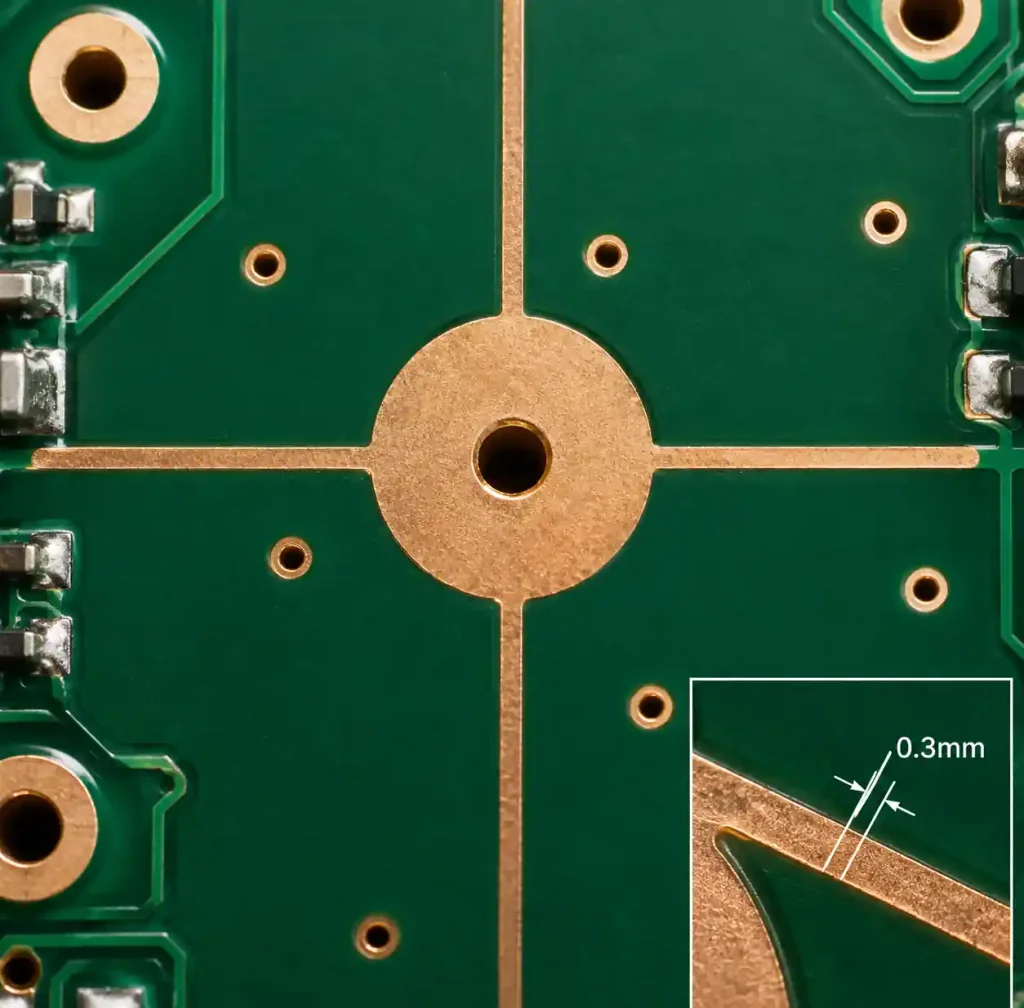
Power planes and heavy copper traces act as heat sinks that prevent proper solder wetting. I’ve seen 4oz copper planes pull so much heat that solder solidifies before complete wetting occurs, creating unreliable cold joints.
Implement thermal relief spokes for all through-hole pads connecting to planes. Use 0.3mm wide spokes—narrower risks breakage during thermal cycling, wider defeats the thermal relief purpose. Four spokes at 90° intervals provide optimal balance between thermal isolation and current capacity.
For connectors with large pins (>1.5mm diameter) on thick copper, extend preheat zone dwell time by 15-20% or increase preheat temperature to 120-140°C. This compensates for thermal mass without pushing wave temperature beyond safe limits for your board material.
Managing Mixed Technology Boards
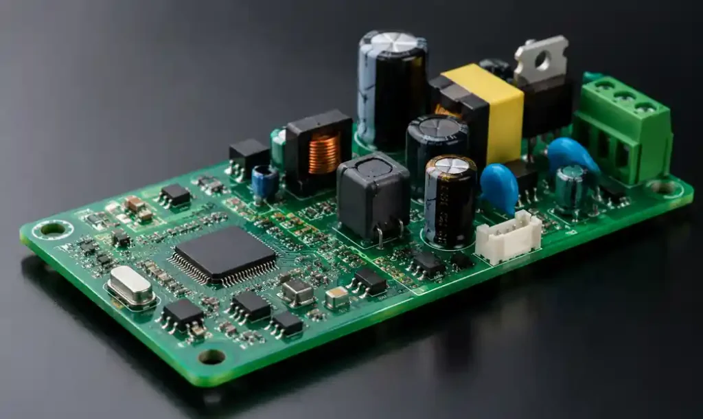
Boards combining SMT and through-hole components demand careful planning. Reflow SMT components first, then wave solder through-hole parts on the bottom side. This sequence prevents exposing delicate SMT packages to wave soldering’s harsh thermal profile.
Protect bottom-side SMT components with selective masking or fixtures. Even components rated for wave soldering temperatures (260°C capable) benefit from protection—we’ve documented 12% reduction in long-term reliability for unprotected bottom-side SMT after wave exposure.
Shadow boards—sacrificial PCBs with cutouts matching SMT component locations—provide mechanical protection and thermal shielding. Dimensi on cutouts 1mm larger than component body to prevent contact while maintaining thermal barriers.
Critical Spacing and Clearance Rules
Minimum clearances prevent bridging while accommodating manufacturing tolerances. These aren’t theoretical numbers—they’re derived from thousands of production panels across different board complexities.
| Feature Pair | Minimum Spacing | Recommended Spacing |
|---|---|---|
| Pad to pad (same net) | 0.6mm | 1.0mm |
| Pad to pad (different nets) | 1.0mm | 1.5mm |
| Component body to pad | 1.5mm | 2.0mm |
| Component to board edge | 3.0mm | 5.0mm |
| Component height difference | N/A | <10mm adjacent |
Increase spacing by 25% for boards using OSP (organic solderability preservative) finish. OSP provides thinner protection than HASL, reducing process margin for bridging prevention.
Fiducial and Tooling Hole Strategy
Wave soldering fixtures require precise PCB registration. Place three non-collinear fiducials on each panel—minimum 1.0mm diameter, bare copper circles with 2.0mm soldermask clearance. Position one fiducial near each corner and a third offset from the diagonal centerline.
Tooling holes enable automated fixture loading. Use 3.2mm diameter NPTH, positioned 5mm from board edges. Three holes in an L-pattern (two on one edge, one on adjacent edge) prevent insertion errors while accommodating assymetric board outlines.
Maintain 8mm keepout zones around tooling holes—no components, vias, or traces. Fixture pins create local stress during clamping that can crack solder joints or damage traces within this radius.
Design for Inspection and Rework
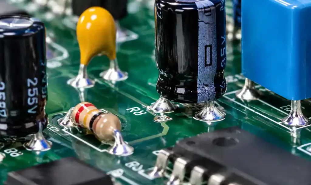
Wave-soldered joints require inspection access. Maintain 2mm clearance between component bodies and adjacent parts to permit automated optical inspection (AOI) cameras to view fillet geometry. For manual inspection, increase this to 3mm to accommodate inspection mirrors and lighting angles.
Design test points on 2.54mm grid spacing, minimum 1.0mm diameter. Place them on the component side when possible to avoid solder coating during wave soldering. If bottom-side placement is unavoidable, add 3mm diameter soldermask dams to prevent solder buildup.
Rework stations need thermal access to component leads. Avoid enclosing through-hole parts with tall mechanical structures or heat-sensitive components. Desoldering a connector next to a plastic mounting boss requires fixture shielding that adds 3-5 minutes per occurrence.
Material Selection Impact on Wave Soldering
Your PCB material affects wave soldering success more than most engineers realize. Standard FR-4 with Tg 130-140°C handles typical wave profiles, but high-layer-count boards (10+ layers) or thick copper (3oz+) benefit from Tg 170°C materials to prevent warpage during the 60-second thermal exposure.
Surface finish selection creates measurable quality differences. HASL (hot air solder leveling) provides excellent wave soldering compatibility—you’re essentially pre-tinning the pads. OSP offers cost advantages but demands tighter process control to prevent bridging. ENIG (electroless nickel immersion gold) works well but costs 30% more than HASL with no wave soldering advantage.
Board thickness influences heat transfer and mechanical stability during wave contact. Standard 1.6mm boards handle most applications, but thin boards (<1.0mm) require fixture support to prevent flexing that causes incomplete wetting. Thick boards (>2.4mm) need extended preheat to achieve uniform thermal distribution.
Common Design Mistakes and Corrections
The most expensive mistake I see is placing high-pin-count connectors with tight pin pitch perpendicular to wave direction. A 40-pin connector with 2.54mm pitch experiences 15-20% bridging rates when oriented incorrectly. Rotate 90° and bridging drops below 1%.
Another frequent error is insufficient thermal relief on ground planes. Engineers forget that ground pins carry no current during wave soldering—they only conduct heat away from the joint. Without thermal relief, ground pins require 2-3x longer contact time to achieve proper wetting, forcing wave temperature increases that damage other components.
Ignoring component height restrictions causes solder shadowing. Mixing 5mm resistors with 20mm capacitors without considering orientation creates defect clusters that AOI catches but fixing requires expensive selective soldering or hand rework.
FAQ
Q: Can I wave solder SMT components on the bottom side?
Not recommended. While technically possible with specific SMT packages rated for wave temperatures, the thermal shock and mechanical stress from the solder wave significantly reduce reliability. Pin-in-paste or selective soldering provides better results for mixed assemblies.
Q: What’s the maximum board thickness for wave soldering?
Standard wave solder equipment handles up to 3.2mm board thickness. Beyond this, preheat becomes insufficient, and fixtures struggle to maintain contact pressure. Heavy copper boards may hit practical limits at 2.8mm due to thermal mass.
Q: How do I prevent solder bridging on fine-pitch connectors?
Use selective soldering instead of wave for connectors below 2.0mm pitch. If wave is required, implement solder thieves (grounded copper traces) between pins to draw away excess solder and increase flux spray pressure by 15%.
Q: Should I use thermal relief for signal layer connections?
Not typically needed unless connecting to large copper pours (>500mm²). Signal traces lack the thermal mass to prevent proper wetting. Over-use of thermal relief weakens mechanical attachment without benefit.
Q: What’s the best way to handle ground pins on connectors?
Always use thermal relief for power and ground pins. Consider increasing spoke width to 0.4mm for high-current ground returns to balance thermal isolation with current capacity.
Q: Can I wave solder after conformal coating application?
No. Conformal coating must occur after all soldering operations. Wave soldering temperatures (250-260°C) exceed the breakdown temperature of all common conformal coating materials, causing outgassing and coating failure.
Conclusion
Wave soldering design rules aren’t arbitrary restrictions—they’re physics-based requirements derived from fluid dynamics, heat transfer, and metallurgy. Master component orientation, respect minimum spacing, implement proper thermal relief, and your boards will achieve first-pass yields above 98%.
The key insight most designers miss is that wave soldering is a system-level process. You can’t optimize pad geometry in isolation or cherry-pick which spacing rules to follow. Every element interacts—your component placement affects thermal management, which influences bridging risk, which determines inspection requirements. Design with the complete process in mind, and wave soldering becomes your competitive advantage instead of your production bottleneck.
At Andwin Circuits, we’ve refined these rules across thousands of board designs and millions of assemblies. Apply them systematically, validate with your CM early in the design phase, and you’ll avoid the expensive lessons learned through production failures.