
High-Speed PCB Design: Impedance Control and Signal Integrity Best Practices
High-speed digital circuits operating above 1 GHz now power 78% of consumer electronics, from smartphones to automotive radar systems. Yet 60% of signal integrity failures trace back to improper impedance control during PCB design and fabrication. When a 50Ω trace measures 54Ω after manufacturing, you lose 0.7dB of signal strength before accounting for via transitions and connector losses—enough to fail USB 3.2, PCIe Gen 4, or DDR5 specifications.
If you want to design high-speed PCBs that meet electrical specifications on the first build, you must understand controlled impedance fundamentals, stackup architecture, trace geometry calculations, and signal return path management. This guide provides practical design rules and manufacturing considerations for circuits from 100 MHz to 28 GHz based on production data from thousands of high-speed designs.
What Is Impedance Control in High-Speed PCB Design?
Impedance control refers to designing PCB traces as transmission lines with predictable characteristic impedance, typically 50Ω for single-ended signals or 85-100Ω for differential pairs. At frequencies where signal rise times produce wavelengths comparable to trace length, every conductor behaves as a transmission line where impedance mismatches create reflections that distort signal integrity.
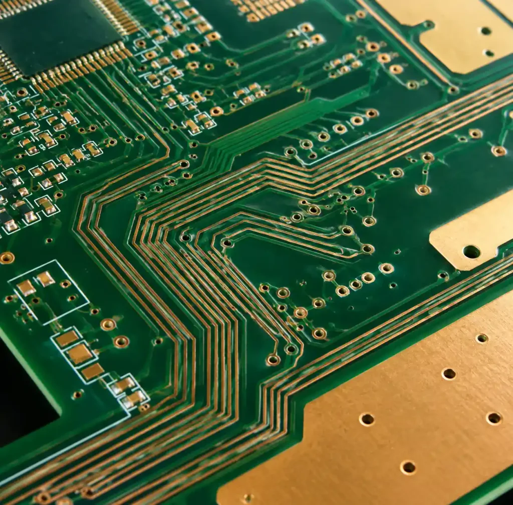
For a 1ns rise time signal, the critical length is approximately 150mm in FR-4 material. Above this length, traces require controlled impedance design to prevent reflections, ringing, and crosstalk. Modern interfaces like USB 3.2 (10 Gbps), HDMI 2.1 (48 Gbps), and DDR5 memory (6400 MT/s) operate with edge rates below 100 picoseconds, making virtually every trace a transmission line requiring impedance control.
According to IPC-2141 standards, controlled impedance tolerance ranges from ±5% for Class 3 applications (aerospace, medical) to ±10% for Class 2 (consumer electronics). You should specify controlled impedance when signal frequencies exceed 50 MHz or rise times drop below 2ns—conditions met by essentially all modern digital interfaces.
Why Signal Integrity Depends on Impedance Matching
Signal integrity failures manifest as eye diagram closure, bit error rate increases, and timing violations. The root cause is impedance discontinuities along the signal path that create reflections. When a signal traveling through a 50Ω trace encounters a 60Ω section, approximately 9% of the signal energy reflects back toward the source, creating ringing that corrupts subsequent bits.
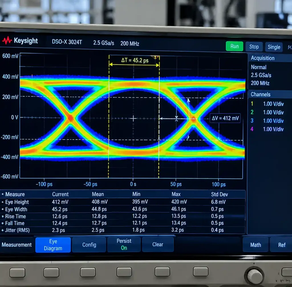
The reflection coefficient equation ρ = (Z₂ – Z₁)/(Z₂ + Z₁) quantifies this effect. A 10Ω impedance step on a 50Ω line produces a reflection coefficient of 0.091, meaning 9.1% voltage reflection. For a 1V signal, this creates 91mV of noise—significant compared to typical 200mV noise margins in 1.8V LVCMOS interfaces.
Cumulative reflections from multiple discontinuities (vias, connectors, package transitions) degrade signal quality further. A high-speed serial link with four 5Ω impedance steps loses 0.8dB insertion loss from reflections alone before considering dielectric and conductor losses. This explains why PCIe Gen 5 (32 GT/s) and USB4 (40 Gbps) demand ±5Ω impedance control across the entire channel.
Critical Parameters Affecting Impedance Control
Four physical parameters determine trace impedance: trace width, dielectric thickness to reference plane, dielectric constant (Dk), and copper thickness. Understanding how each parameter affects impedance allows you to design stackups that meet target impedance values while accommodating manufacturing tolerances.
| Parameter | Effect on Impedance | Typical Tolerance | Design Impact |
|---|---|---|---|
| Trace Width | Wider traces = lower impedance | ±25 μm (±1 mil) | Primary design variable |
| Dielectric Thickness | Thicker dielectric = higher impedance | ±10% | Stackup selection critical |
| Dielectric Constant (Dk) | Higher Dk = lower impedance | ±5% for FR-4, ±2% for Rogers | Material selection matters |
| Copper Weight | Thicker copper = lower impedance | ±10% | Secondary effect |
Trace width provides the most direct impedance control. For 50Ω microstrip on standard 0.254mm (10 mil) dielectric with Dk=4.2, the required trace width is approximately 0.46mm (18 mils). Increasing width to 0.56mm drops impedance to 45Ω; reducing to 0.36mm raises it to 55Ω.
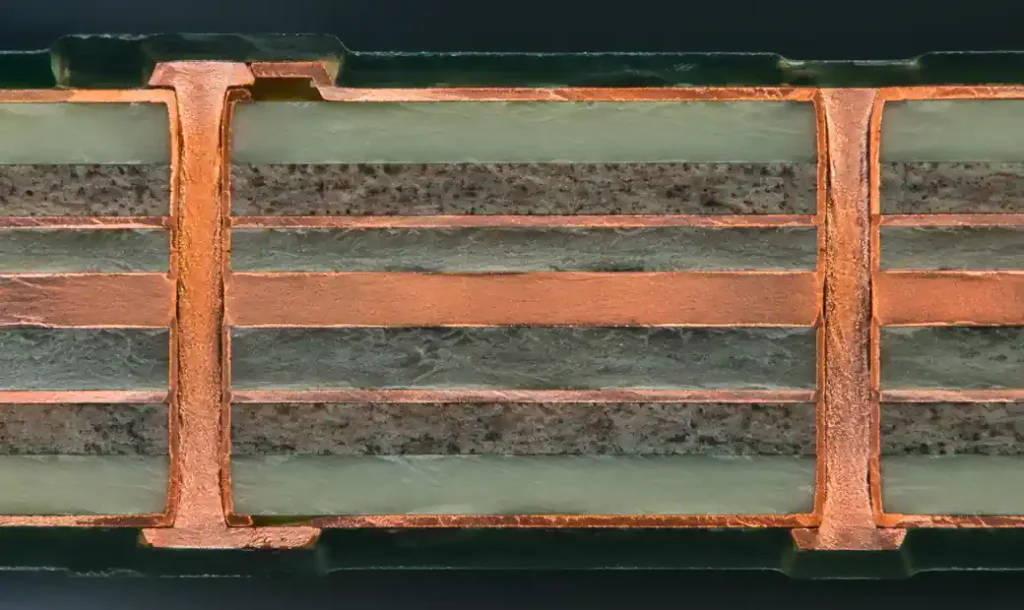
Dielectric thickness variations significantly impact impedance. A ±10% thickness tolerance on 0.254mm core translates to ±5Ω impedance variation on a 50Ω trace. This is why controlled impedance designs specify prepreg and core thicknesses explicitly rather than accepting standard stackup tolerances. Working with advanced multilayer stackups requires precise dielectric thickness control.
Material selection matters for frequency-dependent performance. Standard FR-4 exhibits Dk variation of 4.0-4.5 across frequency and temperature, producing impedance shifts of 3-5Ω. High-frequency materials like Rogers RO4350B maintain Dk=3.48 ±0.05 up to 40 GHz, delivering consistent impedance. Learn more about PCB material properties and their electrical characteristics.
Microstrip vs Stripline Transmission Line Structures
Microstrip and stripline represent two fundamental controlled impedance structures, each with distinct advantages and design trade-offs. Microstrip places the signal trace on an outer layer with a single reference plane beneath it, while stripline sandwiches the signal between two reference planes on internal layers.
Microstrip offers easier routing and component access since traces sit on board surfaces. This structure suits high-speed digital signals requiring test point access or impedance tuning. However, microstrip radiates electromagnetic energy and couples more strongly to adjacent traces compared to stripline. For differential pairs and sensitive analog signals, stripline provides superior noise immunity.
The impedance calculation differs between structures. A 50Ω microstrip on 0.254mm FR-4 (Dk=4.2) requires approximately 0.46mm trace width with 1oz copper. The same 50Ω impedance in stripline with 0.254mm spacing to both reference planes requires only 0.20mm trace width due to dual-plane coupling. This makes stripline more susceptible to fabrication tolerances—a ±25μm width variation affects stripline impedance twice as much as microstrip.
For high-layer-count designs, you can combine both structures strategically. Place high-speed serial interfaces on internal stripline layers for isolation, route clocks and address buses on microstrip for accessibility, and reserve outer layers for power-hungry components requiring thermal dissipation. Understanding layer count optimization strategies helps balance electrical and mechanical requirements.
Designing PCB Stackups for Controlled Impedance
Proper stackup design establishes the foundation for controlled impedance by defining dielectric thickness, reference plane locations, and signal layer assignments. A well-designed stackup ensures every signal has a continuous low-impedance return path while maintaining target impedance values within manufacturing tolerances.
The fundamental rule states every signal layer needs an adjacent reference plane within 0.25mm (10 mils) maximum spacing for frequencies above 1 GHz. This proximity provides low-inductance return current paths and reduces electromagnetic emissions. Six-layer and eight-layer stackups dominate high-speed designs because they provide multiple signal-reference layer pairs while maintaining reasonable board thickness.
A typical 6-layer high-speed stackup arranges layers as: L1 (signals/microstrip) – L2 (ground plane) – L3 (signals/stripline) – L4 (power plane) – L5 (signals/stripline) – L6 (signals/microstrip). This configuration provides three signal layers with excellent reference coupling and power/ground plane capacitance for decoupling.
| Stackup Type | Layer Count | Signal Layers | Advantages | Best Applications |
|---|---|---|---|---|
| Simple 4-layer | 4 | L1, L4 (microstrip) | Low cost, easy to route | <1 GHz, moderate density |
| Standard 6-layer | 6 | L1, L3, L5 or L6 | Good SI, power integrity | 1-10 GHz, mixed signal |
| High-performance 8-layer | 8 | L1, L3, L6, L8 | Multiple stripline, isolation | >10 GHz, DDR4/5, PCIe Gen4+ |
| Advanced 10+ layer | 10-14 | Multiple stripline pairs | Maximum isolation, routing density | 28 GHz+, dense BGA fanout |
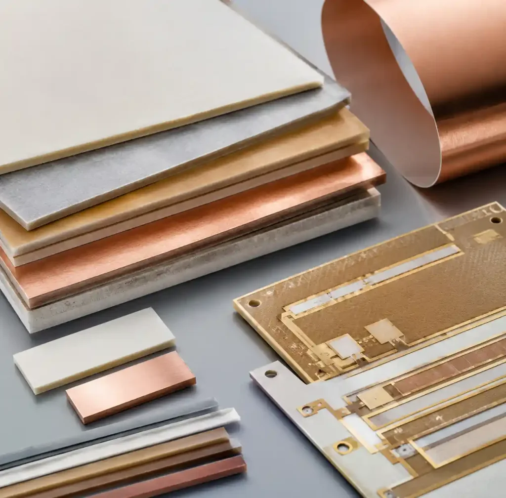
Dielectric selection impacts both impedance and loss. Standard FR-4 works well below 5 GHz with loss tangent (Df) of 0.015-0.020. Above 10 GHz, low-loss materials like Megtron 6 (Df=0.005) or Rogers RO4350B (Df=0.0037) reduce insertion loss by 30-40% compared to FR-4. For high-frequency designs, material selection becomes as critical as trace geometry.
Via Design and Stub Length Management
Vias create impedance discontinuities through three parasitic effects: series inductance from the via barrel, parallel capacitance from the via pad to reference planes, and stub resonance from unused via barrel length. A typical through-hole via on a 1.6mm board exhibits approximately 1nH inductance and 0.5pF capacitance, creating a localized impedance dip that reflects signals above 5 GHz.
The via stub problem affects high-speed designs critically. When a via connects L1 to L4 on an 8-layer board, the unused barrel from L5 to L8 forms a resonant stub. At the stub’s quarter-wave frequency (approximately 15 GHz for a 2mm stub in FR-4), impedance drops to nearly zero, severely degrading signal integrity.
Three techniques eliminate via stubs: back-drilling mechanically removes unused via barrel below the lowest connection layer, blind vias drill only through required layers, and buried vias connect internal layers without reaching board surfaces. Back-drilling represents the most cost-effective solution for through-hole vias, typically adding 10-15% to fabrication cost versus 40-60% premium for blind/buried vias. Learn more about back-drilling for stub removal.
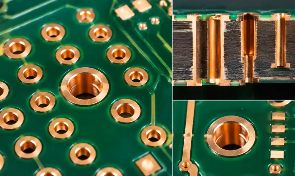
Via-in-pad technology places vias directly beneath BGA or component pads, eliminating trace stubs between pad and via. This technique is essential for high-speed signals above 10 GHz and dense BGA fanout. The via must be filled with conductive or non-conductive epoxy, then capped with copper plating to provide a flat surface for solder joints. Specifications for via-in-pad design rules cover filling, capping, and reliability requirements.
Ground via stitching improves signal integrity by providing multiple return current paths near signal transitions. Place ground vias within 0.5mm of signal vias and space them at λ/20 intervals along high-speed transmission lines—approximately 2-3mm spacing for 10 GHz signals in FR-4. This via fencing technique also reduces crosstalk between adjacent channels by 10-15dB.
Differential Pair Routing Guidelines
Differential signaling dominates modern high-speed interfaces because common-mode noise cancels while differential signals add constructively. USB 3.x, PCIe, HDMI, Ethernet, and MIPI interfaces all use differential pairs with target impedances between 85-100Ω depending on the specific protocol.
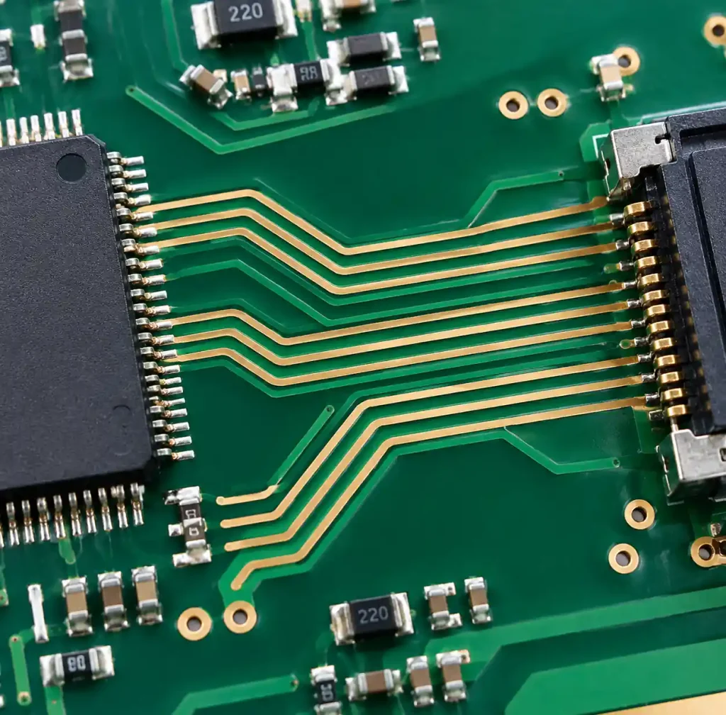
Tight coupling between differential pair traces provides the noise immunity advantage. Space traces at 1-2 times trace width (typically 2-3× width center-to-center spacing) to achieve strong electromagnetic coupling. A 100Ω differential pair on 0.254mm FR-4 requires approximately 0.2mm trace width with 0.2mm spacing between traces—challenging but achievable with modern fabrication.
Length matching within differential pairs maintains timing skew below specification limits. Most high-speed protocols specify maximum intra-pair skew of 5-10 mils (0.127-0.254mm), corresponding to 0.6-1.2 picoseconds timing difference. This tight tolerance demands careful routing with minimal length mismatch between P and N signals.
Keep differential pairs on the same layer to maintain consistent coupling and impedance. Reference plane transitions disrupt the electromagnetic field distribution, creating impedance discontinuities and mode conversion where differential signals partially convert to common-mode noise. When layer changes are unavoidable, place ground via pairs immediately adjacent to signal vias to provide return current paths.
Trace Geometry and Spacing Rules
Minimum trace width and spacing depend on both manufacturing capability and electrical requirements. Standard PCB fabrication supports 4/4 mil (0.1mm) trace and space, adequate for most designs below 5 GHz. High-speed designs often require 3/3 mil or 2.5/2.5 mil capability for dense BGA escape routing and fine-pitch differential pairs.
Crosstalk between adjacent traces increases with proximity and parallel routing length. The 3W rule provides basic isolation: maintain trace spacing of at least three times trace width for parallel routes exceeding 25mm. For critical signals requiring >30dB isolation, increase spacing to 5W or use ground trace isolation between signals.
Trace corners affect impedance at high frequencies. Sharp 90-degree bends create localized capacitance and impedance dips. Use 45-degree chamfered corners or curved traces with radius ≥3× trace width for signals above 5 GHz. Above 20 GHz, specify smooth curves exclusively. Detailed minimum trace width design rules vary by PCB class and application.
Return current follows the path of least impedance directly beneath signal traces. Reference plane splits or gaps force return current to detour, increasing loop inductance and generating EMI. Never route high-speed signals across plane splits. If crossing is unavoidable, place bypass capacitors at the crossing point to provide AC current return paths.
FAQ
What is the standard impedance for high-speed PCB traces?
50 ohms for single-ended signals and 90-100 ohms for differential pairs represent industry standards. USB specifies 90Ω differential, HDMI uses 100Ω, PCIe requires 85Ω, and DDR memory uses 40-60Ω single-ended depending on topology. Always verify specific interface requirements in protocol specifications.
How do I calculate trace width for controlled impedance?
Use field solver calculators from Saturn PCB, Polar Instruments, or your PCB manufacturer’s design tools. Input your stackup parameters including dielectric thickness, dielectric constant, copper weight, and target impedance. Manual calculations using approximation formulas introduce 5-10% error compared to field solvers.
What tolerance should I specify for controlled impedance?
±10% (±5Ω for 50Ω targets) suits most consumer electronics applications per IPC-2141 Class 2. High-reliability designs for medical, aerospace, or data center applications require ±7% or ±5% tolerance. Tighter tolerances increase manufacturing cost by 15-30% due to additional process controls and testing.
When do I need stripline instead of microstrip?
Use stripline for signals requiring maximum isolation from crosstalk and EMI, including sensitive clocks, high-speed serial links above 10 Gbps, and RF circuits. Stripline provides 15-20dB better isolation than microstrip but requires internal routing on 6+ layer boards, increasing complexity and cost.
How does temperature affect impedance control?
FR-4 dielectric constant decreases approximately 0.02-0.03 per 10°C temperature increase, changing 50Ω impedance by 0.5-1Ω across 0-70°C operating range. High-frequency materials like Rogers RO4350B exhibit better thermal stability with <0.3Ω variation over the same temperature range.
What is the maximum via stub length allowed?
Via stub length should not exceed λ/8 at your maximum operating frequency. For 10 GHz signals in FR-4 (wavelength ≈ 10mm), maximum stub length is 1.25mm. Above this length, back-drilling or blind/buried vias become necessary to prevent stub resonance affecting signal integrity.
Conclusion
High-speed PCB design success depends on understanding and implementing controlled impedance principles from initial stackup planning through final fabrication. Proper impedance control requires coordinated attention to trace geometry, stackup architecture, via design, and material selection—all working together to maintain signal integrity across multi-gigabit interfaces.
The practices outlined in this guide—50Ω and 100Ω target impedances, proper microstrip and stripline calculations, via stub management, differential pair coupling, and careful stackup design—represent proven approaches validated across thousands of production designs operating from 1 GHz to 28 GHz.
If you need high-quality controlled impedance PCBs for your high-speed design project, Andwin Circuits offers advanced manufacturing capabilities up to 50 layers with ±5% impedance tolerance. Our testing includes TDR verification on every production lot and fast 7-day delivery for quick-turn prototypes. Contact us today for controlled impedance PCB manufacturing with guaranteed electrical performance and factory-direct pricing.