
Minimum Trace Width and Spacing: Design Rules by PCB Class
A 3mil/3mil trace-and-space design on Class 3 medical devices costs 45-60% more than 5mil/5mil equivalents, yet most hardware teams default to tighter geometries without cost-benefit analysis. IPC-2221 and IPC-6012 define minimum trace width and spacing by PCB class, but real manufacturing capabilities vary dramatically from baseline standards to advanced HDI processes.
IPC Classification System: What Each Class Means
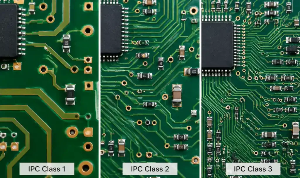
IPC-2221 and IPC-6012 establish three performance classes that determine trace geometry limits, fabrication tolerances, and inspection criteria.
Class 1 products include consumer electronics and non-critical applications where cosmetic defects are acceptable and product life rarely exceeds 1-2 years. Minimum conductor spacing starts at 0.1mm (4 mils) for voltages under 50V. Trace width minimums typically range from 0.15mm (6 mils) for signal traces.
Class 2 covers most commercial electronics including computers, industrial controls, and telecommunications equipment requiring 3-5 year service life. Conductor spacing tightens to 0.075-0.1mm (3-4 mils). Trace widths drop to 0.1-0.125mm (4-5 mils) for signals, demanding tighter process control and automated optical inspection.
Class 3 serves high-reliability applications: medical devices, automotive systems, aerospace, and military hardware where failure consequences are severe. Minimum spacing remains 0.075mm but with zero tolerance for defects. Class 3 adds 15-25% to fabrication costs through enhanced inspection and lower yield acceptance thresholds.
Standard vs Advanced PCB Capabilities
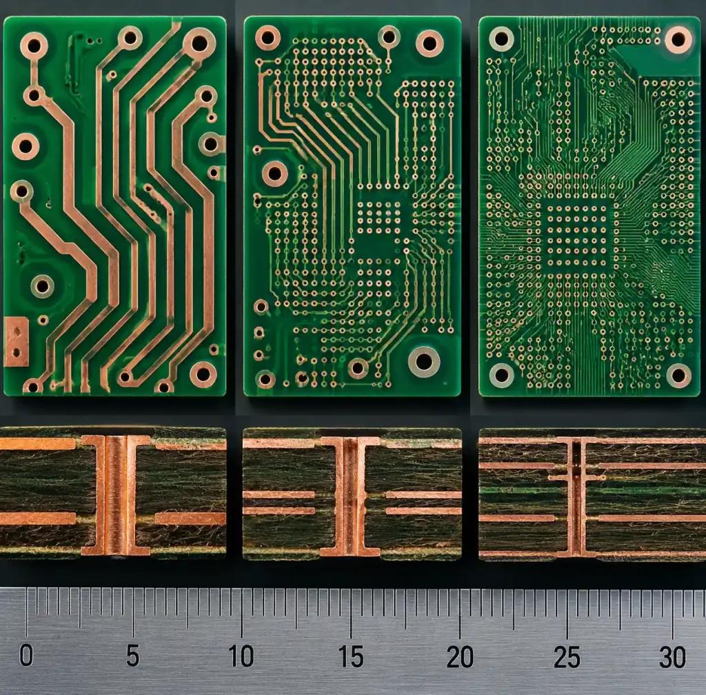
Manufacturing capabilities split into standard and advanced tiers based on line formation technology, imaging resolution, and etching control. Standard capabilities serve Class 1-2 products while advanced processes enable Class 3 and HDI designs.
Standard capability boards use photoimaging with 50-75μm resolution and wet etching that achieves 0.1-0.125mm (4-5 mil) traces reliably. Most manufacturers offer these as baseline services with 5-7 day lead times.
Advanced capability processes employ laser direct imaging (LDI) at 15-25μm resolution, enabling 0.075mm (3 mil) and finer geometries. Some facilities achieve 0.05mm (2 mil) traces using modified semi-additive processes (mSAP) borrowed from HDI manufacturing.
| Capability Tier | Minimum Trace/Space | Imaging Technology | Cost Premium | Lead Time Impact |
|---|---|---|---|---|
| Standard | 0.125mm (5 mil) | Film photoimaging | Baseline | 5-7 days |
| Fine Line | 0.1mm (4 mil) | LDI | +15-25% | +2-3 days |
| Advanced | 0.075mm (3 mil) | LDI + precision equipment | +35-50% | +4-6 days |
| HDI/mSAP | 0.05mm (2 mil) | LDI + specialized chemistry | +60-120% | +7-10 days |
Process yield drops as geometries tighten. A 0.125mm design achieves 95-98% yield while 0.075mm falls to 85-92%, making aggressive trace widths expensive at prototype volumes.
Trace Width and Current Carrying Capacity
IPC-2221 nomographs relate conductor cross-sectional area, current, and temperature rise. Actual capacity depends on trace length, ambient temperature, copper weight, and layer position.
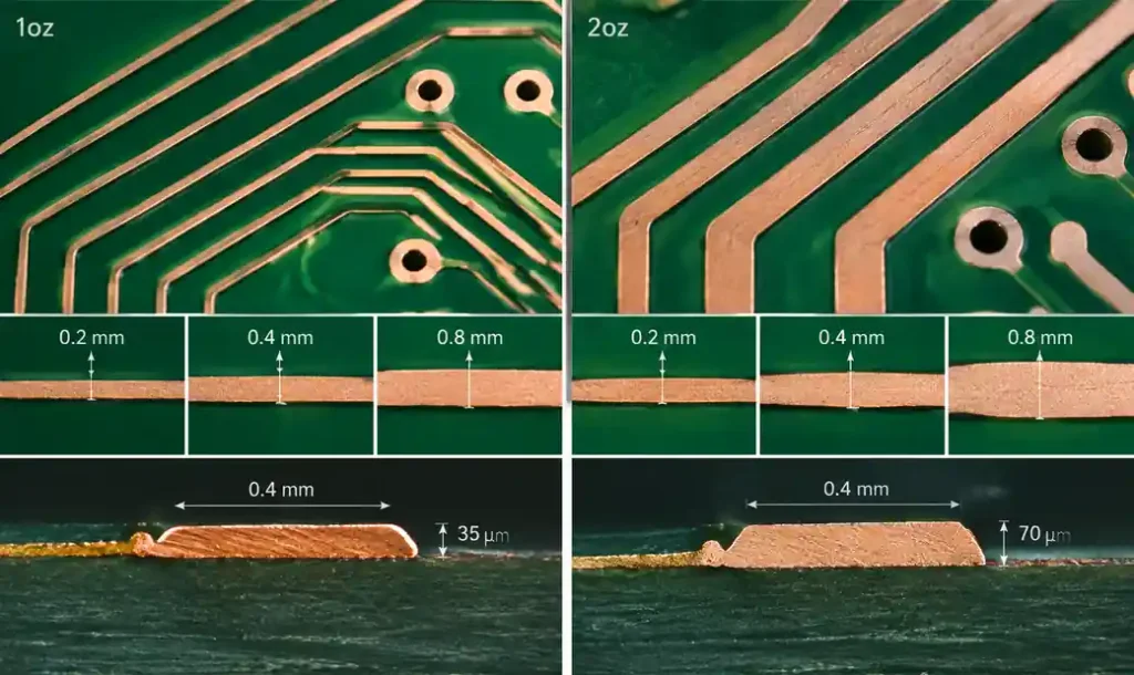
External layers benefit from direct air convection and handle 30-40% more current than internal traces. A 0.25mm (10 mil) trace in 1oz copper on an outer layer carries approximately 1.0-1.3A with 10°C temperature rise at 25°C ambient.
Copper weight directly impacts current capacity. 2oz copper doubles thickness from 35μm to 70μm, allowing 60-70% higher current in the same trace width but costs 20-35% more due to longer plating cycles.
| Trace Width | 1oz Cu Outer (10°C Rise) | 1oz Cu Inner (10°C Rise) | 2oz Cu Outer (10°C Rise) | Design Guideline |
|---|---|---|---|---|
| 0.1mm (4 mil) | 0.4A | 0.3A | 0.7A | Signals only |
| 0.125mm (5 mil) | 0.5A | 0.4A | 0.9A | Low-current power |
| 0.25mm (10 mil) | 1.2A | 0.8A | 2.0A | Standard power |
| 0.5mm (20 mil) | 2.4A | 1.7A | 4.0A | Medium power |
| 1.0mm (40 mil) | 4.8A | 3.5A | 8.0A | High current |
Derate current capacity by 20-30% for safety margin. A trace carrying 2A continuous should be sized for 2.5-2.6A capacity to account for manufacturing variations and thermal cycling. Power electronics designs often require thermal analysis beyond IPC-2221 when traces exceed 3-4A.
Controlled Impedance Impact on Trace Geometry
Controlled impedance routing for high-speed signals adds geometric constraints beyond minimum fabrication limits. A 50-ohm single-ended trace or 100-ohm differential pair requires specific width-to-height ratios that often exceed minimum trace capabilities.
Microstrip traces on outer layers typically need 0.125-0.2mm (5-8 mil) width for 50-ohm impedance on standard 1.6mm boards. Going narrower to 0.1mm raises impedance to 60-70 ohms unless you reduce dielectric thickness, which impacts stackup design.
Stripline configurations bury traces between ground planes where copper weight variations have greater impedance impact. A ±0.0125mm width variation causes ±3-4 ohm impedance shift. Class 3 boards specify ±10% impedance tolerance, requiring width control of ±0.013mm or better.
Differential pairs add spacing requirements. 100-ohm pairs typically need 0.15mm (6 mil) traces with 0.1mm (4 mil) spacing on outer layers. Tightening to 0.1mm traces with 0.075mm spacing adds 15-20% to costs through enhanced process control.
Cost Implications of Fine-Line Designs
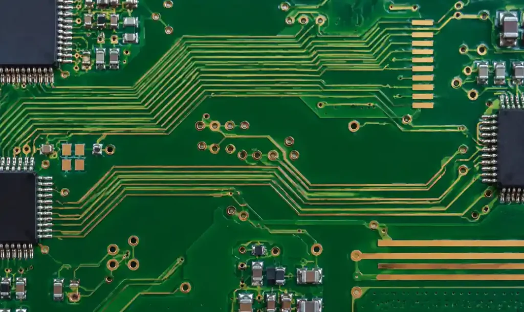
Trace geometry directly impacts manufacturing yield, tooling requirements, and inspection complexity.
Moving from 5mil/5mil to 4mil/4mil increases fabrication costs by 15-25%. Tighter line widths require LDI equipment ($800K-$1.5M capital investment), pulse plating tanks, and automated measurement systems.
At 3mil/3mil specifications, cost premiums reach 35-50% versus 5mil baseline. Yield losses become significant—scrap rates climb 8-12 percentage points from open circuits or bridging defects.
Sub-3mil geometries using mSAP cost 60-120% more than standard designs. While enabling 2mil/2mil or finer, mSAP requires specialized facilities with cleanroom environments and extended 12-15 day processing cycles.
Volume considerations: At production quantities above 5,000 units, fine-line cost premiums compress to 10-15% through tooling amortization. Prototype orders under 100 units bear full premium costs.

Voltage Spacing Requirements Beyond Manufacturing Limits
IPC-2221 Table 6-1 specifies minimum conductor spacing based on peak operating voltage, separate from fabrication capabilities. These electrical clearance requirements often exceed manufacturing minimums.
For voltages 0-50V, minimum spacing is 0.13mm (5.1 mils) externally and 0.1mm (4 mils) internally. Most Class 2 designs operate in this range.
Between 51-100V, required spacing jumps to 0.4mm (15.7 mils) externally and 0.1mm (4 mils) internally. At 101-150V, external spacing reaches 0.5mm (19.7 mils) while internal layers require 0.2mm (7.9 mils).
| Voltage Range | External Spacing | Internal Spacing | Typical Application |
|---|---|---|---|
| 0-50V | 0.13mm (5.1 mil) | 0.1mm (4 mil) | Logic, low voltage |
| 51-100V | 0.4mm (15.7 mil) | 0.1mm (4 mil) | Power supplies |
| 101-150V | 0.5mm (19.7 mil) | 0.2mm (7.9 mil) | Industrial control |
| 151-300V | 0.8mm (31.5 mil) | 0.4mm (15.7 mil) | High voltage systems |
Industrial control applications operating at 300-400VAC require 1.5-2.0mm creepage distances, far exceeding manufacturing limitations. These boards use dedicated high-voltage zones with guard traces and conformal coating.
Design Margin Recommendations by Application
Designing to absolute minimums creates manufacturing challenges and reliability risks. Optimal margins vary by application context and volume projections.
Prototype and low-volume designs (under 500 units annually) benefit from conservative 5mil/5mil or 6mil/6mil geometries. Wider traces reduce fabrication cost, shorten lead times, and improve yields at facilities without advanced capabilities.
Consumer electronics targeting 10,000+ unit volumes justify tighter 4mil/4mil designs when board area directly impacts enclosure size and material costs. A 15% board area reduction can offset the 20% fabrication premium.
Class 3 medical and automotive products demand reliability over density. These designs typically maintain 5mil/5mil minimums with 6mil/6mil preferred spacing despite Class 3 permitting 3mil. The margin protects against copper thickness variations, registration errors, and thermal cycling effects.
High-frequency designs above 1GHz often use 4-5mil traces for controlled impedance matching rather than density. The manufacturing challenge shifts to maintaining consistent width across the panel (±0.0125mm tolerance) for impedance control within ±7%.
FAQ
What is the minimum trace width for Class 2 PCBs?
Class 2 boards typically support 0.1mm (4 mil) minimum trace width, though 0.125mm (5 mil) provides better manufacturing margins and costs less.
How much current can a 10-mil trace carry?
A 10-mil (0.25mm) trace in 1oz copper on an outer layer carries approximately 1.2A with 10°C temperature rise. Always derate by 20-30% for design margin.
Does Class 3 require finer traces than Class 2?
No. Class 3 uses the same minimum dimensions as Class 2 (0.1mm/4 mil) but enforces stricter inspection criteria and zero defect tolerance—increasing cost without changing geometry.
Why do fine-line PCBs cost more?
Sub-5mil designs require laser direct imaging equipment, pulse plating, tighter process control, and additional inspection. Yield losses from defects add 15-50% costs depending on geometry.
When should I use 3mil/3mil trace spacing?
Use 3mil only when board area constraints mandate maximum density or HDI via-in-pad routing is required. Most designs achieve adequate performance with 4-5mil spacing at lower cost.
How does copper weight affect minimum trace width?
Heavier copper creates steeper etching sidewalls requiring wider compensation. Practical minimums: 1oz copper = 4 mil, 2oz = 5 mil, 3oz = 6 mil, 4oz = 8 mil for reliable manufacturing.
What spacing is required for 110VAC mains voltage?
IPC-2221 requires 0.5-0.8mm (20-31 mils) for 110VAC depending on conformal coating. Always consult the full voltage/spacing table and safety standards for your specific application.
Can I mix trace widths on the same PCB?
Yes. Use minimum widths only where density demands require it. Power traces, ground planes, and less-critical signals should use wider geometries (6-10 mil) for better current capacity and lower cost.
Conclusion
Minimum trace width and spacing decisions impact manufacturing cost, reliability, and electrical performance significantly. IPC-2221 and IPC-6012 establish baseline minimums of 0.1mm (4 mil) for Class 2-3 boards, but optimal design geometry balances fabrication capability against cost and yield risks. Standard 5mil/5mil designs deliver the best cost-performance ratio for most commercial applications. Tighter 4mil or 3mil geometries add 15-50% fabrication costs while requiring advanced processes. These aggressive specifications make sense only when board area reduction justifies the premium or HDI routing density is mandatory. Focus design optimization on routing efficiency and stackup planning rather than pushing trace geometries to limits.