
Power Supply PCB Design: Layout Best Practices for Switching Regulators
Power supply failures account for 35% of PCB-related field returns, most from layout mistakes. When designing buck converters or boost regulators above 100 kHz, layout becomes the circuit—not just component arrangement.
I’ve debugged supplies that met electrical specs but radiated 15 dB over limits or exhibited 200 mV ripple instead of 20 mV. The difference? Layout decisions that turned parasitic inductance into failures. To pass EMC testing on first build, understand current loop management, ground strategy, and thermal considerations.
What Makes Switching Regulator Layout Different?
Switching regulators create pulsed waveforms with rise times under 10 ns. At 500 kHz, fast edges make every trace a transmission line. A 10mm trace adds 10 nH parasitic inductance—generating 5V spikes when 10A switches in 10 ns, from V = L(di/dt).
The hot loop—the high di/dt path where energy switches between input capacitor, high-side FET, low-side FET, and ground—operates at full switching current with nanosecond rise times. Minimize its area or accept radiated EMI that fails compliance.
Input Capacitor Placement: The 5mm Rule
Position input bulk capacitors within 5mm of the switching IC’s VIN and PGND pins. This capacitor sources instantaneous current when the high-side switch closes—5-10A in mobile applications or 50A+ in servers.
Every millimeter adds inductance converting switching current into voltage spikes. For 5A switching in 8ns, even 5nH generates a 3V spike from L(di/dt). These spikes stress FETs, radiate EMI, and couple into feedback causing instability.
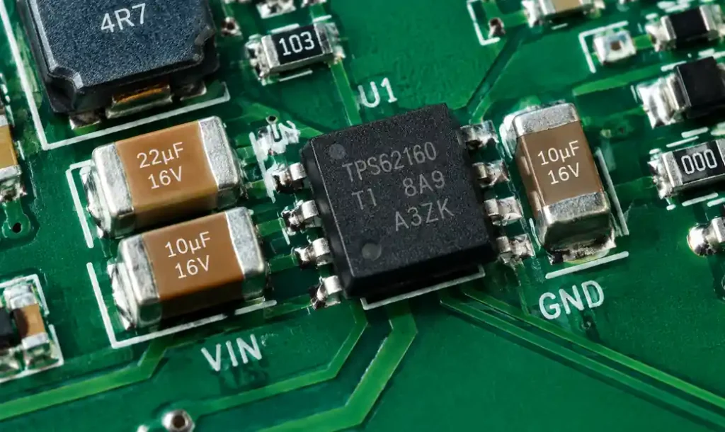
Use ceramic capacitors with X7R or X5R dielectrics, never Y5V which loses 80% capacitance at rated voltage. For a 12V buck delivering 3A, place 22µF ceramic at VIN with ground returning to PGND through the shortest path. Add 10µF if input exceeds 20V or frequency exceeds 1 MHz.
| Input Voltage | Load Current | Input Capacitance | Max Trace Length |
|---|---|---|---|
| 5V | 1-3A | 22µF ceramic | 5mm |
| 12V | 3-5A | 22µF + 10µF | 3mm |
| 24V | 5-10A | 47µF ceramic | 3mm |
| 48V | 10A+ | 47µF + 22µF | 2mm |
Route the capacitor ground pad directly to the IC’s power ground—not through shared ground plane. This dedicated connection prevents switching current from flowing through analog ground and coupling noise into feedback.
Switching Node Area Minimization
The switching node—connecting high-side FET, low-side FET, and inductor—carries full load current with voltage edges slewing at 5-20 V/ns. This node radiates broadband noise from tens to hundreds of MHz.
Keep switching node copper under 20 mm² for <5A designs and under 50 mm² for 10A+. Use minimum copper area satisfying current density—typically 1 oz copper at 1A per 10 mil width for 10°C rise.
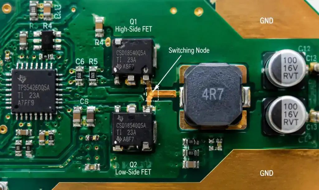
Never extend switching node traces to other board sections. Route input capacitors, FETs, and inductor in tight cluster with <5mm traces. For integrated FET controllers, place inductor within 3mm of SW pin.
Use ground plane cutouts beneath switching nodes to prevent capacitive coupling increasing common-mode EMI. A 2mm clearance provides isolation without excessive return path impedance.
Ground Plane Strategy
Split or unified? Control where high-frequency switching currents return. For basic buck converters without integrated analog, unified ground works with intelligent placement. Position output capacitor so its ground return connects between low-side FET ground and load ground, ensuring ripple current flows through capacitor without passing IC analog ground pins.
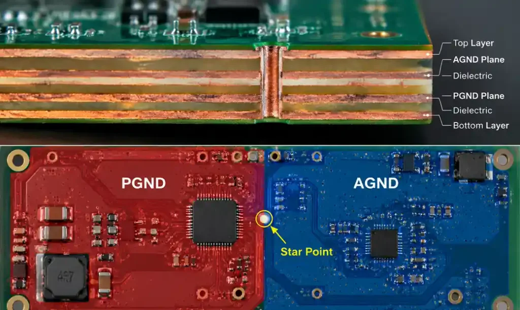
For designs integrating analog control, sensitive feedback, or multi-phase topologies, implement power ground (PGND) and analog ground (AGND). Connect at a single point—typically at IC’s central pad or power ground pin. Route all switching currents through PGND, while feedback and compensation use AGND.
| Ground Strategy | Topology | Advantages | Considerations |
|---|---|---|---|
| Unified ground | Single-phase buck/boost | Simple, low impedance | Requires careful placement |
| Split ground (star) | High-precision, low-noise | Isolates analog from power | Can increase EMI if poor |
| Dual-plane + stitching | Multi-phase, integrated ADC | Balance isolation/impedance | Via placement critical |
Never route high-speed digital or analog traces across split ground planes. Signals crossing splits create undefined return paths generating emissions and susceptibility.
Feedback Trace Routing
Feedback networks connect to high-impedance inputs (1 MΩ+), making them noise-sensitive. Route feedback on quiet layers—never on switching node layer. Place feedback divider within 10mm of output capacitor positive terminal. Use ground plane beneath for shielding.
Connect ground side to IC’s AGND, not noisy power ground. Add 10-100 pF across upper feedback resistor creating low-pass filter attenuating noise without affecting DC regulation. See more about PCB layer stackup design.
Thermal Management for MOSFETs
For surface-mount MOSFETs in SO-8, DPAK, or PowerPAK packages, PCBs act as primary heat sinks. Design large copper pours (minimum 500 mm²/watt) beneath FET packages. Use thermal vias (minimum 8 vias, 0.3mm diameter) connecting thermal pad to internal ground planes.
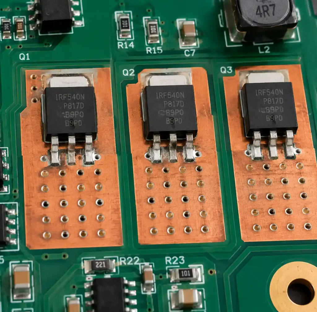
For 1oz copper, 1W dissipation targeting 30°C rise requires 2,333 mm². Add 30% margin. For advanced thermal management, consider metal-core substrates.
| Package | θJA (°C/W) | Copper Area (mm²/W) | Min Vias |
|---|---|---|---|
| SO-8 (exposed pad) | 40-50 | 1,000 | 6 |
| DPAK (TO-252) | 25-35 | 700 | 8 |
| PowerPAK SO-8 | 30-40 | 800 | 8 |
| D2PAK (TO-263) | 20-25 | 500 | 10 |
Position inductors away from heat-sensitive components. Allow minimum 5mm clearance. Learn about heavy copper PCB design.
EMI Reduction Techniques
Layout-based EMI reduction starts with loop area minimization but extends to shielding and filtering. These techniques reduce radiated emissions by 20-30 dB without expensive filters.
Input filtering: Add common-mode choke and X-capacitor at power input blocking differential and common-mode noise. Position before other circuitry, with ground connecting to chassis if available.
Via stitching: Place grounded vias at 5mm intervals around power supply perimeter creating “fence” preventing RF coupling to adjacent circuits. Effective above 50 MHz where vias act as low-impedance connections.
Guard traces: Route grounded traces on both sides of sensitive paths (feedback, analog sensing) for shielding. Connect to ground at multiple points using vias spaced at λ/10 intervals, ~30mm at 100 MHz.
Spread spectrum: Many controllers offer frequency dithering spreading switching harmonics across ±10% range. This reduces peak emissions by 8-12 dB without affecting efficiency, easing conducted emissions testing below 30 MHz. For comprehensive EMI control strategies, consider ESD protection integration.
Route output cables away from switching node area. Use twisted pairs for outputs exceeding 100mm, creating field cancellation reducing radiated emissions.
Current Loop Analysis
Identify three critical loops:
Hot loop (highest priority): Input cap → High-side FET → Low-side FET → Ground return. Carries full switching current with nanosecond rise times. Minimize to <100 mm² for <5A buck converters.
Output loop: Inductor → Output cap → Load → Ground return. Carries continuous but pulsating current at switching frequency. Prioritize placement for thermal coupling to load.
Feedback loop: Output sense → Feedback divider → IC FB pin → IC ground → Output ground. High-impedance and noise-sensitive. Route away from switching nodes using shielded layers.
For multi-phase regulators, each phase has its own hot loop. Position input capacitors to service all phases with equal impedance, typically in phase array center.
Heavy Copper Considerations
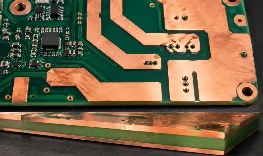
Standard 1oz copper suffices for <10A. Above this, consider 2oz or heavy copper for power traces.
Heavy copper reduces DC resistance. A 100mm trace at 15A:
- 1oz (2.5mm wide): 13.4 mΩ, 3W dissipation, 30°C rise
- 2oz (2.5mm wide): 6.7 mΩ, 1.5W dissipation, 15°C rise
Heavy copper increases cost by 40-80%. Use selectively for power planes. For >30A, consider metal-core PCBs.
Output Capacitor Placement
Position output capacitors within 10mm of inductor and load connection. Output capacitors filter inductor ripple and supply load transients.
Use low-ESR ceramics (X7R, X5R) in parallel. Typical 12V, 3A buck uses 22µF + 10µF providing <10mΩ ESR at 500kHz.
Calculate minimum: Cout = (Iload × D) / (fsw × Vripple)
For 3A, 40% duty, 500kHz, targeting 20mV: Cout = 120µF
Ceramic derating reduces capacitance by 40-60%, so specify 220µF nominal. Reference our PCB assembly services.
Layer Stack Recommendations
Four-layer boards represent minimum for >2A regulators:
- Layer 1: Signal and components
- Layer 2: Ground plane (solid)
- Layer 3: Power plane
- Layer 4: Signal and components
Continuous ground on Layer 2 provides low-impedance return paths and shields between power and signal. Route hot loop entirely on Layer 1 with ground directly beneath.
For high-power (>10A) or mixed-signal requiring <5mV noise, use six layers adding isolated analog ground and dedicated quiet signal layer.
FAQ
Q: Can I use 2-layer PCB for switching regulators?
Yes, for <2A at 5V with non-critical EMI. Use generous copper pours and route hot loop on top with ground pour beneath. Expect 10-15% worse efficiency and higher EMI versus 4-layer due to increased ground impedance.
Q: How much clearance around switching node?
Maintain 2mm between switching node and sensitive analog signals. For >40V, increase to 0.5mm per 100V following IPC-2221 spacing. Add ground plane cutout with 2mm clearance preventing capacitive coupling.
Q: Should feedback be differential?
Not necessarily. Single-ended works if traces <50mm, routed over ground plane with local bypassing. Use differential only for >50mm routing or extremely noisy environments (>10V/m EMI susceptibility).
Q: Can multiple supplies share ground planes?
Yes, but connect thoughtfully. Each supply’s hot loop should return through dedicated ground area, then join at single star point—typically at input connector or central ground node. This prevents one supply’s current from flowing through another’s feedback network.
Q: What causes EMC testing failures?
Common culprits: input/output cables as antennas (use common-mode chokes, ferrite beads), inadequate input filtering (add X2/Y capacitors), ground plane discontinuities (check splits forcing current detours), poor chassis grounding (connect PCB to enclosure at multiple points using <30mm connections).
Conclusion
Successful switching regulator layout begins with minimizing hot loop area—placing input capacitors, FETs, and inductor in compact cluster with <5mm traces. Separate power ground from analog ground or control return paths through intelligent placement. Route feedback away from switching nodes with ground plane shielding beneath. Size copper and add thermal vias managing heat, targeting junction temperatures below 100°C under maximum load. These fundamentals deliver stable regulation, manageable EMI, and thermal performance meeting requirements from first prototype.