
Depanelization Methods: V-Cut vs Tab Routing vs Laser Cutting
PCB depanelization represents a critical manufacturing step where improper technique selection causes 15-20% of assembly damage in high-volume production. Studies show that mechanical stress from separation accounts for up to 30% of post-assembly failures in sensitive components like BGAs and 01005 passives.
If you want to choose the right PCB depanelization method for your assembly project, then you will need to understand the mechanical stress characteristics, edge quality requirements, and cost implications of each separation technique. This comprehensive guide compares V-cut scoring, tab routing, and laser cutting to help you optimize manufacturability and product reliability.
What is PCB Depanelization?
PCB depanelization is the mechanical or thermal process of separating individual printed circuit boards from a manufacturing panel after assembly. The panel format improves SMT assembly efficiency by processing multiple boards simultaneously, but separation introduces mechanical stress that can damage components, crack solder joints, or delaminate board materials.
You can use depanelization methods ranging from manual breaking along V-grooves to automated laser cutting systems. The selection depends on board outline complexity, component edge clearance, production volume, and acceptable stress levels for assembled components.
V-Cut (V-Scoring) Depanelization
Process and Mechanism
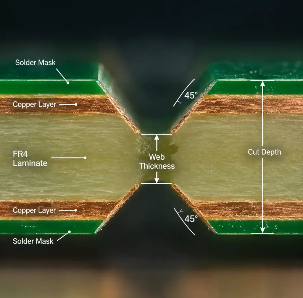
V-cut depanelization uses circular blades to create V-shaped grooves on both sides of the panel along straight separation lines. The blades remove material to a depth of 1/3 to 2/3 of the board thickness, leaving a web thickness of 0.3-0.5mm that allows boards to be separated by manual or machine-assisted snap-off.
The V-groove angle typically ranges from 30° to 60°, with 45° being most common for 1.6mm thick FR4 boards. This geometry creates a controlled fracture line that propagates through the remaining material during separation.
Advantages and Limitations
V-cut offers the fastest separation speed at 10-15 boards per minute for automated systems, making it cost-effective for high-volume production. The process requires no additional tooling cost beyond blade maintenance and produces minimal edge debris when properly executed.
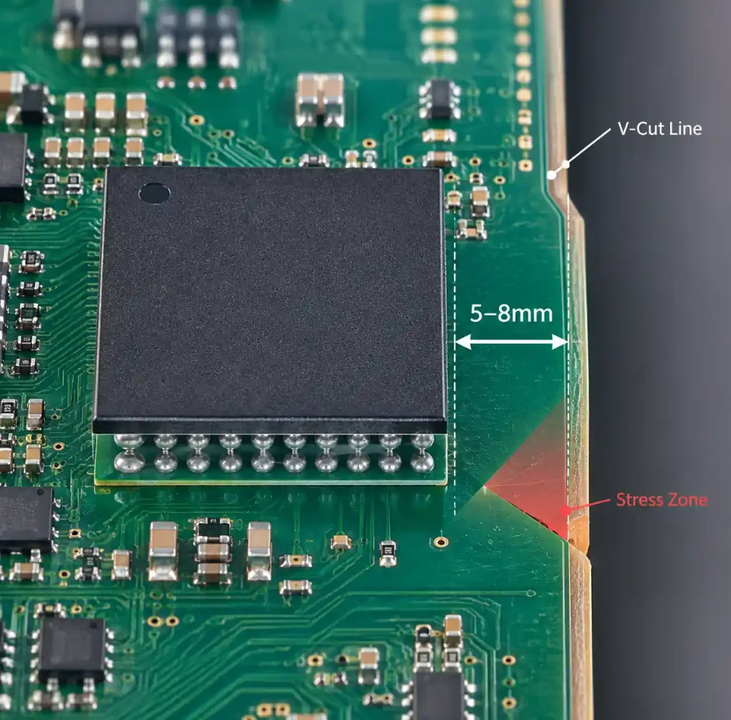
However, V-cut works only for straight-line separations with rectangular or square board outlines. The method induces higher mechanical stress (estimated 40-60% higher than routing) because separation relies on bending force applied perpendicular to the score line. This stress propagates 5-8mm from the separation edge, requiring component keep-out zones.
Design Requirements
You should maintain minimum 5mm component clearance from V-cut lines for standard passive components and 8mm for stress-sensitive parts like BGAs. Board thickness must be between 0.8mm and 3.2mm for reliable V-scoring, with thicker boards requiring wider V-angles to prevent incomplete fracture.
The residual web thickness determines separation force: 0.4-0.5mm webs need 3-5kg force while 0.3mm webs separate with 1-2kg force. Thinner webs reduce mechanical stress but increase risk of premature separation during panel handling.
Tab Routing Depanelization
Process and Mechanism
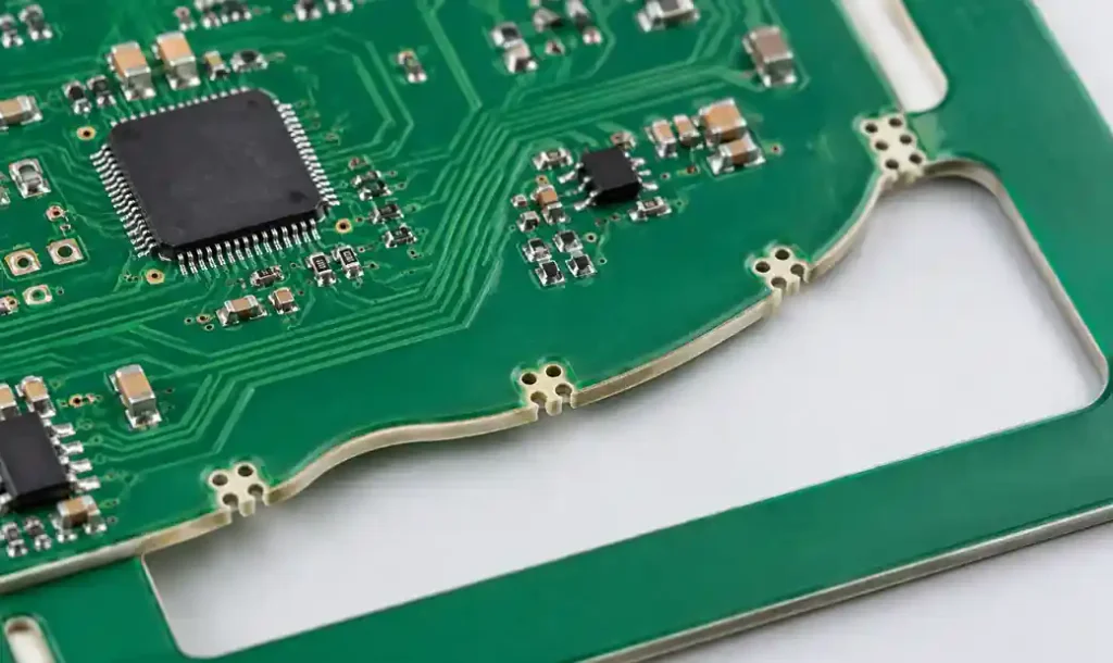
Tab routing creates perforated outlines using CNC routers or mechanical milling, connecting individual boards to the panel frame through small tabs (mouse bites). The tabs typically measure 1-3mm in width and 0.5-1.5mm in length, providing mechanical support during assembly while allowing controlled break-off afterward.
Routing depth equals the full board thickness, producing true board contours without the geometric limitations of V-scoring. Tab placement and quantity determine separation force and residual stress distribution.
Advantages and Limitations
Tab routing supports any board outline geometry, including circular, irregular, and complex shapes with internal cutouts. The method distributes mechanical stress across multiple small break points rather than one continuous line, reducing peak stress concentration by 40-50% compared to V-cut.
Separation speed ranges from 3-6 boards per minute depending on tab count and board outline complexity. The process leaves small tab remnants on board edges that may require secondary finishing for applications demanding smooth edges. Edge quality shows roughness of 50-100μm without post-processing.
Design Requirements
You should place tabs every 50-80mm along routed edges for 1.6mm thick boards, with more frequent spacing for thinner or larger boards. Minimum tab width should be 1.5mm for boards up to 2mm thickness and 2-3mm for heavier copper or thick core constructions.
Component keep-out zones need only 2-3mm from routed edges since separation stress concentrates at tab locations rather than along the entire perimeter. Tab remnants extend 0.3-0.8mm from the designed board edge, which must be considered in enclosure fit calculations.
Laser Depanelization
Process and Mechanism
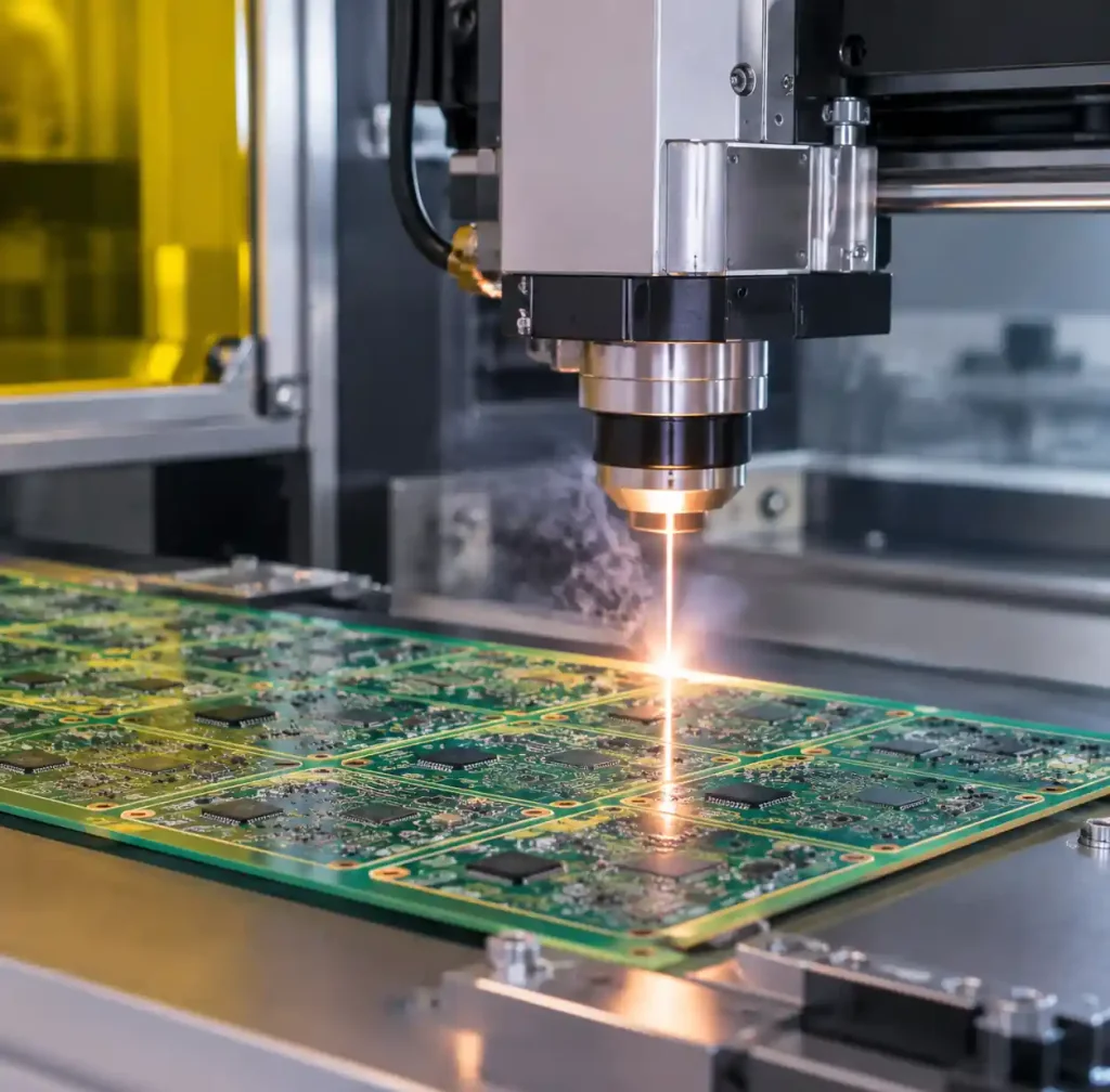
Laser depanelization uses CO₂ or UV laser systems to ablate board material along separation lines through localized thermal energy. CO₂ lasers (10.6μm wavelength) vaporize organic materials like FR4 while UV lasers (355nm wavelength) provide finer cut width for applications requiring minimal heat-affected zones.
The process creates cut widths of 0.05-0.15mm depending on laser type and power settings, with virtually zero mechanical stress transmission to assembled components. Multi-pass cutting prevents excessive thermal buildup that could damage nearby components or board materials.
Advantages and Limitations
Laser cutting produces the cleanest edge quality with roughness below 20μm and no mechanical stress on components. The method supports any board outline geometry with higher precision than routing, making it suitable for flex circuits, thin boards (0.2-0.8mm), and assemblies with components placed close to board edges.
Separation speed is slower at 1-3 boards per minute, and equipment cost ranges from $50,000-$200,000 compared to $8,000-$25,000 for routing systems. The process generates carbonization at cut edges and requires fume extraction systems for organic material vaporization.
Design Requirements
You can place components as close as 0.5-1mm from laser-cut edges since thermal effects remain localized within 0.2-0.3mm of the cut line. The method works well for boards from 0.2mm to 3mm thickness, though cutting speed decreases significantly for materials thicker than 2.5mm.
Laser power must be optimized for board construction: too low power requires multiple passes increasing cycle time, while excessive power causes charring, delamination, or pad lifting near board edges. Material compatibility should be verified as some flame retardants produce excessive smoke or residue during laser ablation.
Depanelization Method Comparison
| Parameter | V-Cut | Tab Routing | Laser Cutting |
|---|---|---|---|
| Board Outline | Straight lines only | Any geometry | Any geometry |
| Separation Speed | 10-15 boards/min | 3-6 boards/min | 1-3 boards/min |
| Mechanical Stress | High (bending force) | Medium (tab breaking) | Minimal (thermal) |
| Component Clearance | 5-8mm required | 2-3mm required | 0.5-1mm acceptable |
| Edge Quality | 100-200μm roughness | 50-100μm roughness | <20μm roughness |
| Equipment Cost | $5,000-$15,000 | $8,000-$25,000 | $50,000-$200,000 |
| Operating Cost | $0.02-0.05/board | $0.05-0.10/board | $0.15-0.30/board |
| Board Thickness | 0.8-3.2mm | 0.4-6mm | 0.2-3mm |
| Secondary Finishing | Not required | Optional (tab removal) | Not required |
Stress Impact on Component Reliability
Mechanical Stress Analysis
V-cut separation introduces bending moments of 15-25 N·mm at the score line, creating tensile stress on the component side and compressive stress on the solder side. This asymmetric loading can crack solder joints on large components like BGAs where the package corner exceeds 5mm from the board neutral axis.
Tab routing distributes separation force across multiple discrete points, reducing peak stress by 40-50%. However, tabs positioned too close to component pads can still transmit localized stress that weakens solder fillets or lifts pads from the substrate.
Laser cutting eliminates mechanical stress entirely but introduces thermal gradients of 150-250°C within 0.2-0.3mm of the cut line. Components placed closer than 1mm may experience localized heating that softens solder joints or thermally stresses moisture-sensitive plastic packages.
Component-Specific Considerations
You should use laser cutting or routing for assemblies with 01005 and 0201 passive components where the entire component body sits within 2mm of the board edge. These ultra-small parts have minimal mass to resist mechanical shock and crack easily under V-cut bending stress.
BGAs and LGAs require minimum 8mm clearance from V-cut lines to prevent corner ball cracking. For routing, 3-4mm clearance suffices if tabs are positioned away from BGA corners. Laser cutting permits BGA placement as close as 2mm from board edges when thermal management is properly controlled.
Heavy components (>2g) need additional consideration regardless of depanelization method. Their inertia during panel separation can generate forces exceeding solder joint strength, particularly when multiple heavy components align near the separation line. Routing with carefully positioned tabs provides the best balance of speed and stress control for such assemblies.
Cost Analysis by Production Volume
| Production Volume | Recommended Method | Rationale |
|---|---|---|
| <500 boards | Manual V-cut or routing | Low equipment amortization |
| 500-5,000 boards | Automated V-cut (straight) or routing (complex) | Balanced cost and flexibility |
| 5,000-50,000 boards | Automated routing or laser (high reliability) | Process consistency critical |
| >50,000 boards | V-cut (simple outlines) or laser (complex/high-reliability) | Full automation justifies capital cost |
For prototype and low-volume production under 500 boards per month, manual V-cut separation or hand routing with tabs offers the lowest total cost. Equipment investment remains minimal and labor cost stays below $0.10 per board for simple geometries.
Medium-volume production (5,000-50,000 boards per year) benefits from automated routing systems that handle complex outlines at reasonable throughput. The $8,000-$25,000 equipment cost amortizes to $0.15-$0.40 per board over 2-3 years depending on utilization rate.
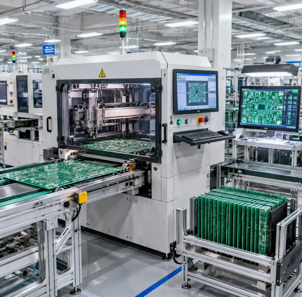
High-volume production exceeding 50,000 boards per year justifies laser depanelization investment when component reliability or edge quality requirements prohibit mechanical methods. Equipment cost amortizes to $0.20-$0.50 per board over 5 years, with reduced rework and failure costs offsetting the higher initial investment.
Selection Framework for Design Engineers
Decision Tree Approach
Start by evaluating board outline geometry: if all separation lines are straight and orthogonal, V-cut offers the fastest and most economical solution provided component placement meets the 5-8mm clearance requirement.
For boards with curved, circular, or irregular outlines, choose between routing and laser based on component edge clearance. If all components maintain >3mm clearance from board edges, routing provides adequate quality at moderate cost. When components must be placed within 1-2mm of edges, laser cutting becomes necessary despite higher operating cost.
Consider component sensitivity as the second decision factor. Assemblies with stress-sensitive parts like crystal oscillators, MEMs sensors, or ceramic capacitors >0603 size benefit from laser or careful routing over V-cut regardless of outline geometry.
Application-Specific Recommendations
Consumer electronics with high production volume and rectangular boards should use automated V-cut for optimal cost efficiency. The method supports throughput demands while keeping separation cost under $0.05 per board.
Medical devices and automotive electronics requiring IPC Class 3 reliability need routing or laser depanelization to minimize mechanical stress on solder joints. The reduced failure rate justifies higher separation costs when field failures carry significant warranty or safety implications.
Wearable devices and IoT products with circular or irregular PCB shapes require routing or laser cutting by default. Laser cutting works particularly well for these applications since miniaturization often forces components close to board edges where routing tabs would interfere with assembly density.
Frequently Asked Questions
What is the minimum board thickness for V-cut depanelization?
V-cut works reliably for boards 0.8mm and thicker. Thinner boards tend to crack unpredictably during separation because the remaining web thickness becomes too small to control fracture propagation. For boards below 0.8mm, use routing or laser cutting instead.
Can laser depanelization cut through metal core PCBs?
Standard CO₂ and UV lasers cannot cut aluminum or copper base materials used in metal core PCBs. These require mechanical routing or specialized fiber laser systems operating at higher power densities. Most MCPCB applications use routing with tabs for separation.
How does depanelization method affect conformal coating?
V-cut and routing can crack conformal coating along separation edges if the coating extends into the cut zone. Apply conformal coating after depanelization or use selective coating to avoid the separation area. Laser cutting can burn through some coating materials, requiring post-cut cleaning or coating repair.
What is the typical equipment lifespan for each method?
V-scoring blades require replacement every 50,000-100,000 cut inches depending on board thickness and material. Routing bits last 20,000-50,000 inches before dimensional accuracy degrades. Laser systems need mirror cleaning every 2,000-5,000 hours and tube replacement every 10,000-20,000 hours of operation.
How do you prevent board warpage during depanelization?
Support the panel uniformly during separation to distribute stress evenly. For V-cut, use fixtures that clamp the board 10-15mm on both sides of the score line. Routing and laser systems should support the panel perimeter with minimal clamping force to avoid inducing bow or twist during the process.
Can you combine depanelization methods on the same panel?
Yes, hybrid approaches use V-cut for main separation lines and routing or laser for complex cutouts or internal openings. This optimizes cost by using fast V-cut where possible while maintaining design flexibility for irregular features. Ensure the V-cut and routing depths are coordinated to prevent premature separation.
Conclusion
Choosing the right depanelization method requires balancing mechanical stress, production speed, edge quality, and cost against specific application requirements. V-cut delivers optimal efficiency for high-volume rectangular boards with standard component clearances. Tab routing provides design flexibility for irregular outlines at moderate cost and stress levels. Laser cutting minimizes mechanical and thermal stress for high-reliability applications where component placement density demands close edge proximity.
If you need PCB assembly services with optimized depanelization for your production volume and design requirements, Andwin Circuits offers comprehensive panelization design support and automated depanelization equipment up to 50-layer manufacturing capability. Our DFM analysis ensures your panel design matches the selected separation method for maximum reliability and cost efficiency. Contact us today for custom PCB assembly solutions with factory-direct pricing and fast delivery in 7 days for prototypes.