
Industrial Motor Drivers: Heavy Copper and Metal Core PCB Solutions
When designing PCBs for industrial motor drivers, inverters, and VFDs, FR4 often doesn’t cut it. We’ve seen too many boards cook themselves or drop voltage under load because the copper couldn’t handle the current or the heat had nowhere to go. High current demands—20A to 200A continuous, with startup peaks over 500A—push standard PCBs to their limits. This guide walks through heavy copper and metal core PCB options, with design rules and material selection guidance we actually use on the job.
Why Motor Driver PCBs Need Special Solutions
Motor control circuits are brutal on PCBs. MOSFETs and IGBTs dump heat, gate drivers add their share, and the copper traces have to carry serious current without overheating. Standard 1 oz copper would need traces wider than your board to handle 50A with a reasonable temperature rise. Heavy copper PCBs (3–20 oz) solve the current problem by putting more copper in the same footprint.
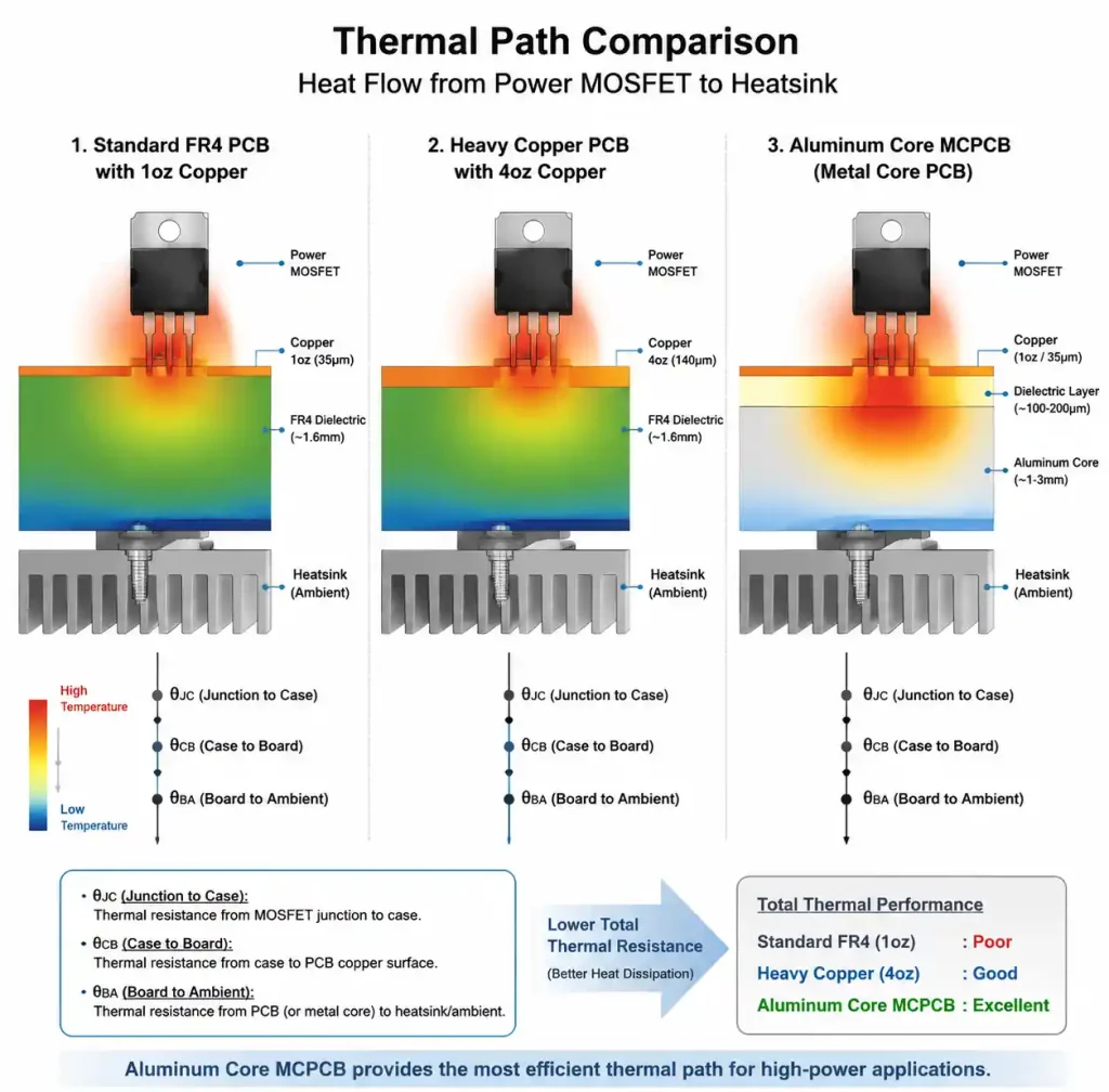
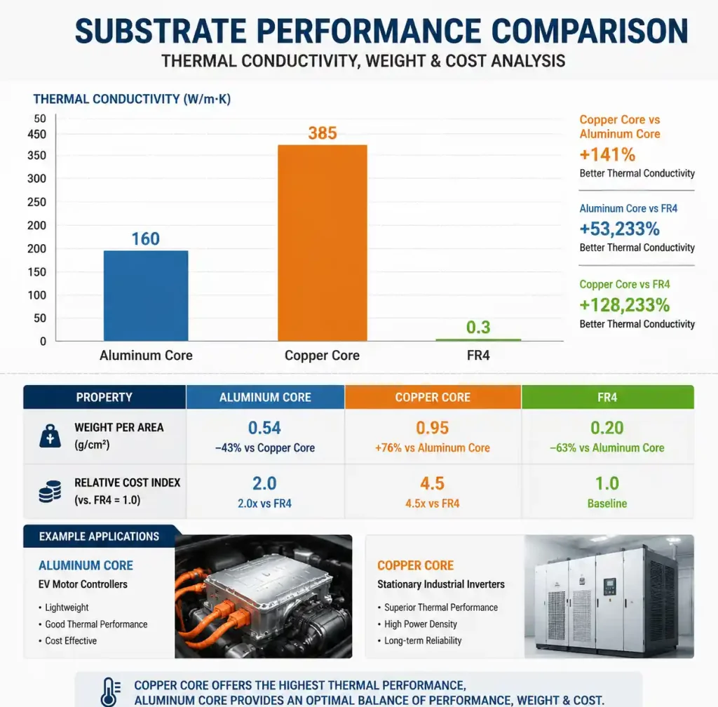
Metal core PCBs swap the FR4 core for aluminum or copper, giving you 5–10× better thermal conductivity. For motor driver designs that need both high current and good heat dissipation, hybrid stackups with heavy copper on metal core are increasingly common. When comparing substrate options, our aluminum PCB vs metal core PCB guide helps clarify which thermal solution fits your power density requirements.
The real question isn’t which technology to use—it’s how much current and how much heat you’re dealing with, and what your budget can handle.
Heavy Copper PCB vs Standard PCB: Key Design Parameters
Heavy copper means 3 oz (105 µm) or more on one or more layers. Standard PCBs use 0.5–2 oz. More copper means higher current capacity, better heat spreading, and mechanical toughness—but etching gets trickier. Minimum trace width and spacing go up as copper weight increases because of undercut during the chemical etch process.
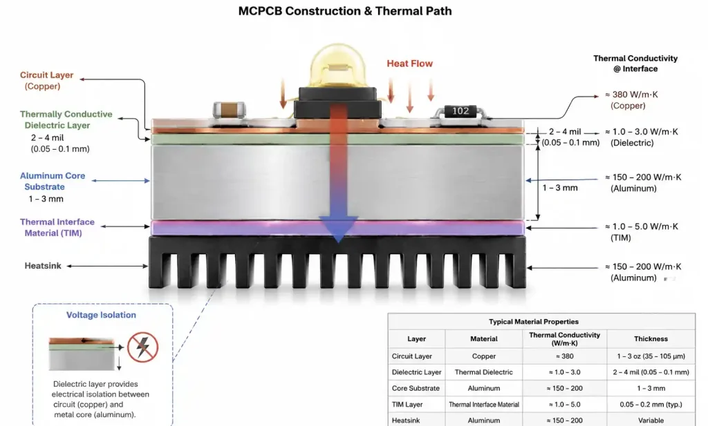
For a given trace width, current capacity scales roughly linearly with copper thickness. A 10 mm wide trace at 1 oz carries about 5A with a 10°C rise. The same trace at 4 oz handles 20A. The downside: 4 oz copper needs 8–10 mil spacing versus 4–5 mils for 1 oz.
Table 1: Heavy Copper vs Standard Copper Design Rules
| Parameter | 1 oz | 3 oz | 4 oz | 6 oz |
|---|---|---|---|---|
| Finished thickness | 35 µm | 105 µm | 140 µm | 210 µm |
| Min trace width | 4 mil | 8 mil | 10 mil | 12 mil |
| Min spacing | 4 mil | 8 mil | 10 mil | 12 mil |
| Current capacity (10mm trace, 10°C rise) | ~5A | ~15A | ~20A | ~30A |
| Via fill | Optional | Recommended | Required | Required with plating |
For motor driver layouts, keep signal layers at 1 oz to preserve routing density, and dedicate heavy copper to power planes or outer layers. And remember: thicker copper spreads heat better. A 4 oz plane has about 4× the in-plane thermal conductivity of 1 oz, which can cut junction-to-ambient thermal resistance by 15–25%.
Metal Core PCB Technology for Thermal Management
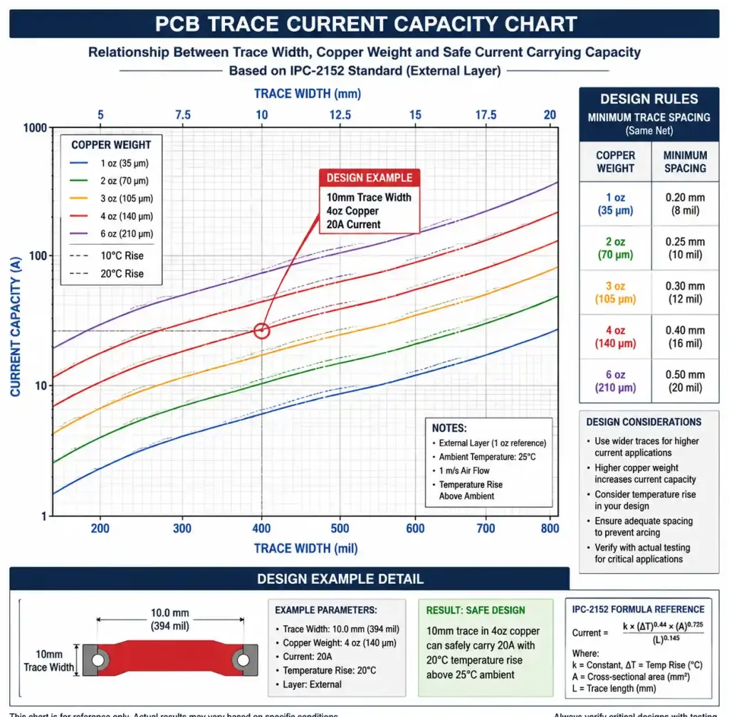
MCPCBs replace the FR4 core with aluminum (or copper) bonded to the circuit layer through a thermally conductive dielectric. The metal core gives you a direct path to a heatsink—junction-to-case thermal resistance can drop to 0.5°C/W with proper mounting.
The critical parameter is the dielectric layer. Typical materials run 2–10 mils thick with thermal conductivity of 1.5–5 W/m·K. Thinner dielectrics transfer heat better but reduce voltage isolation. For motor drivers on 400–800 VDC buses, you need to balance thermal performance against creepage and clearance per IPC-2221.
Table 2: MCPCB Dielectric Options for Motor Drivers
| Dielectric Type | Thickness | Thermal Conductivity | Dielectric Strength | Best For |
|---|---|---|---|---|
| Standard epoxy | 4 mil | 1.5 W/m·K | 3 kV | Low-voltage (<100V) |
| High-thermal epoxy | 3 mil | 3.0 W/m·K | 2.5 kV | Medium-power BLDC |
| Ceramic-filled | 4 mil | 4.0 W/m·K | 4 kV | 400–800V inverters |
| Polyimide | 2 mil | 2.5 W/m·K | 3.5 kV | Compact high-density |
For 400 VDC bus, a 4 mil ceramic-filled dielectric gives you both good thermal conductivity (4 W/m·K) and enough breakdown margin. For sub-60V designs, a thinner 2–3 mil dielectric gets you better heat transfer.
Most MCPCBs are single-layer, but double-layer constructions exist. Single-layer puts all components on top; double-layer adds routing flexibility but needs thermally conductive via fill.
Combining Heavy Copper with Metal Core
For the tough jobs—3-phase inverters driving 50+ HP motors—heavy copper on MCPCB gives you current capacity and thermal management in one board. Typical hybrid stackups use 3–4 oz copper on the circuit layer of an MCPCB.
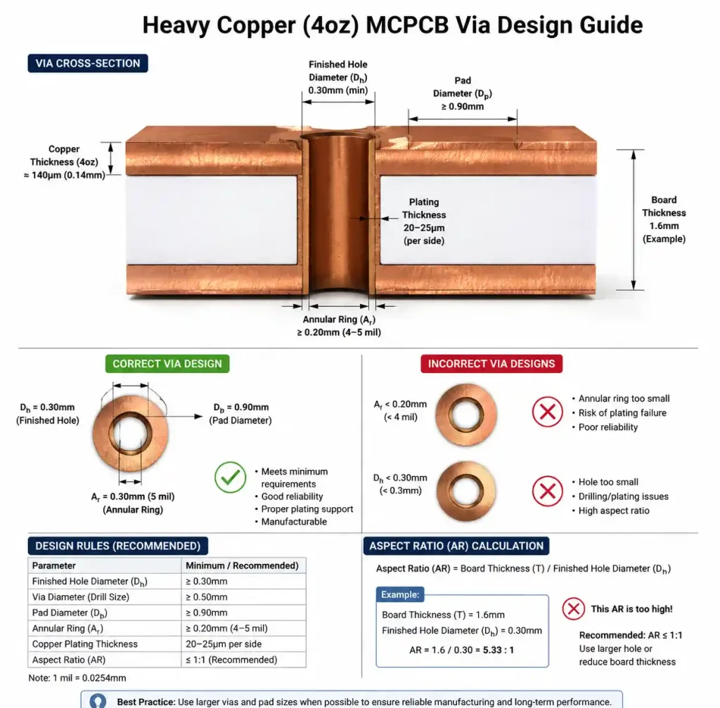
The trick is via aspect ratio. With 4 oz copper (140 µm) on 4 mil dielectric over 2 mm aluminum core, vias need careful sizing. Minimum via diameter should be 0.5 mm with 0.3 mm finished hole to get reliable plating. And don’t tent thermal vias—exposed vias couple heat to the core better.
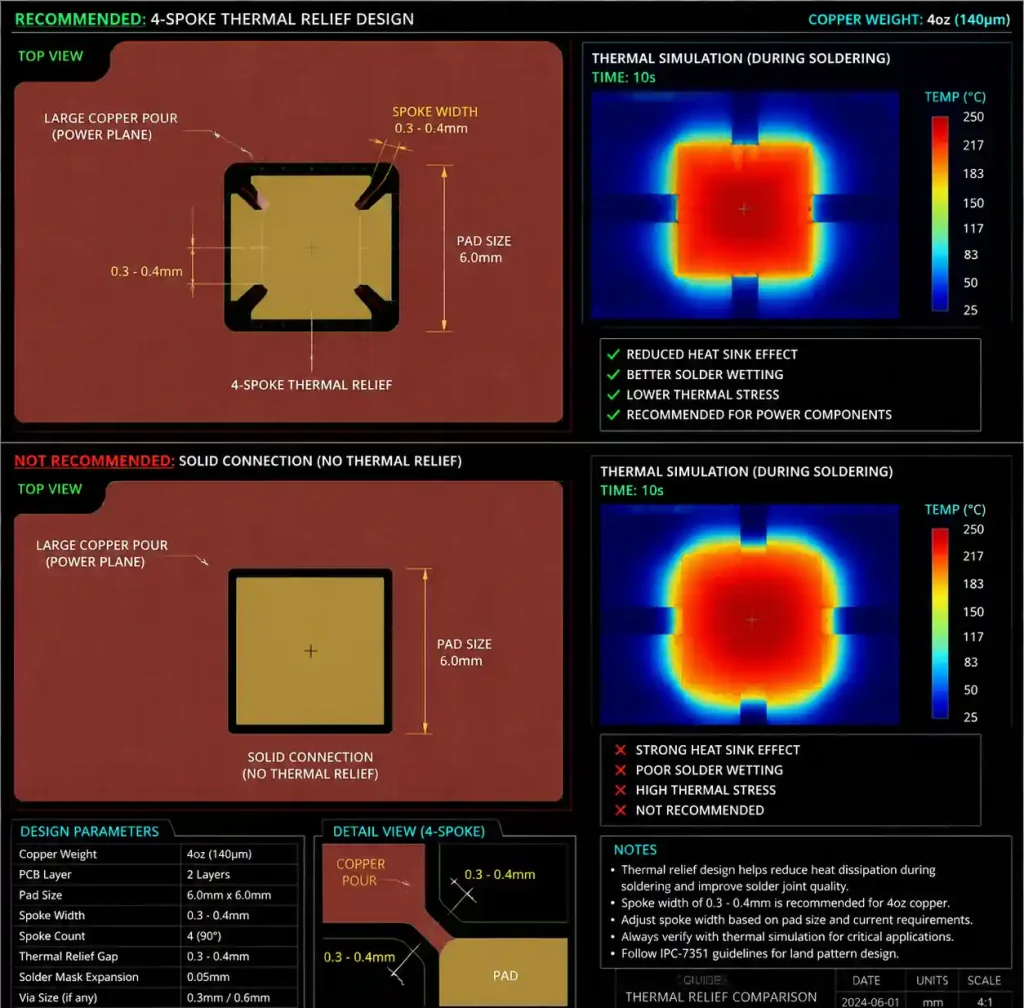
Thermal expansion mismatch between copper (17 ppm/°C) and aluminum (23 ppm/°C) matters. Large copper pours parallel to board edges can crack over thermal cycles. Break up big copper areas with thermal relief spokes and keep continuous traces under 100 mm where possible.
DFM Considerations for High-Current PCBs
Heavy copper and MCPCBs come with manufacturing quirks. Common DFM issues we see: insufficient spacing for etch undercut, skimpy annular rings, thermal relief problems, and panelization oversights.
Heavy copper etching undercuts about 1.5–2× the copper thickness. For 4 oz (140 µm), expect 200–280 µm of undercut—your 0.25 mm designed gap might become 0.10 mm after etching. Add 4–5 mils to spacing beyond Table 1 values.
Annular ring needs bumping up too. IPC-6012 Class 2 asks for 2 mil minimum, but we target 4–5 mils for heavy copper to handle drilling tolerance and plating. For 0.3 mm vias in 4 oz copper, use 0.7–0.8 mm pad diameter.
Thermal relief is critical. Solid connections from pads to large copper pours act like heat sinks, making soldering difficult. Use 4-spoke reliefs with 0.3–0.4 mm spoke width for 4 oz copper. For through-hole power terminals over 50A, go direct solid connection.
Panelization: aluminum core can’t be scored or V-grooved like FR4. Use tab routing or stamp holes. Route 3 mm minimum tab width for boards over 100×100 mm, with at least 4 tabs to prevent warping.
FAQ
Q: What copper weight for a 100A motor driver?
For 100A continuous, spec 4–6 oz on power layers. A 15 mm trace in 4 oz copper handles 100A with about 20°C rise. For transients above 100A, 6 oz gives extra thermal mass. Above 150A, consider bus bars or parallel traces.
Q: Can I mix 1 oz and 4 oz copper in one stackup?
Yes—hybrid stackups are common. Outer layers at 4 oz for power, inner layers at 1 oz for signals and controlled impedance. It optimizes cost vs performance. Tell your fab early so they adjust lamination parameters.
Q: What’s the minimum creepage for 600 VDC on MCPCB?
IPC-2221 says 6.4 mm for Material Group IIIa, or 5.0 mm for Group II dielectrics (typical MCPCB). We recommend 7–8 mm for real-world margin—contamination and altitude derating happen. Surface coating can reduce creepage but requires process validation.
Q: How do I calculate MCPCB thermal resistance?
Device datasheet gives θJC. Case-to-board (θCB) depends on pad, solder, dielectric—typical 0.5–2°C/W. Board-to-ambient (θBA) depends on core thickness, mounting, TIM. For aluminum MCPCB on a heatsink, θBA is roughly 0.2–1.0°C/W. Total θJA = θJC + θCB + θBA.
Q: Should I use solder mask over heavy copper traces?
Usually no—solder mask adds thermal resistance and can crack from expansion mismatch. For 4 oz power traces, leave copper exposed with ENIG or immersion silver. Use solder mask dams between adjacent traces to prevent bridging during assembly.
Conclusion and Next Steps
Heavy copper and MCPCBs are must-haves for industrial motor drivers where current and heat are deal-breakers. For 3-phase inverters, VFDs, and servo drives, our rule of thumb: 4 oz or heavier for traces above 20A, MCPCB when junction temps start creeping up on FR4, and dielectric thickness matched to your bus voltage.
Before sending Gerbers, check your spacing rules for heavy copper, verify annular ring margins, and confirm thermal relief design on power pads. For 400+ VDC, double-check creepage and clearance per IPC-2221. When working with high-density via structures in thick copper layers, following blind and buried via design rules helps ensure your vias stay reliable through thermal cycling and reflow.
If you want a second set of eyes on your stackup or DFM, upload your design files—we’ll run a free review and flag any heavy copper or MCPCB issues before you commit to fabrication. For production verification, our flying probe vs fixture testing guide can help you choose the right test strategy for your motor driver boards.