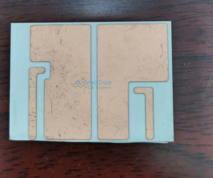
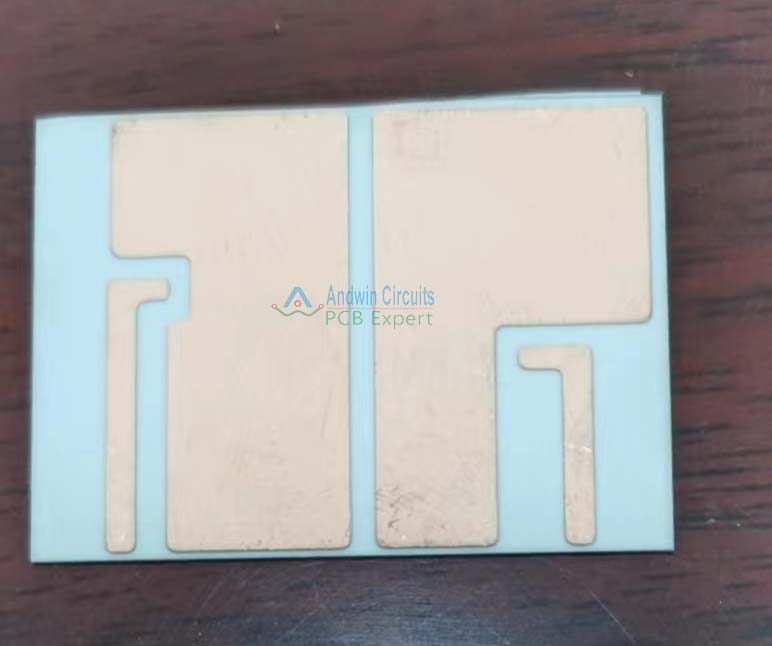
AMB Silicon nitride (SI3N4) Ceramic PCB: The Ultimate Solution for High-Performance Electronics
AMB Silicon nitride (SI3N4) Ceramic PCB: The Ultimate Solution for High-Performance Electronics
What is AMB Silicon nitride (SI3N4) Ceramic PCB?
AMB is active metal brazing technology.
The AMB ceramic PCB is a type of printed circuit board that uses a ceramic PCB substrate instead of
the traditional fiberglass or epoxy substrate.
AMB technology is a further development of DBC technology.
It is a method of combining ceramics and metals by using active metal elements (such as Ti/Ag/Zr/Cu) in solder.
Ceramics form a reactive layer that can be wetted by liquid solder.
The bonding in the AMB ceramic substrate is achieved by the chemical reaction of the ceramic
And the active metal solder at temperature,
And the Si3N4 ceramic used in the AMB has a higher thermal conductivity (>90W/mK)
Compared to the traditional Al2O3 ceramic substrate 25°C),
Which is closer to the thermal expansion coefficient of silicon (2.6×10 -6 /K).
Therefore, the AMB substrate has high adhesive strength and reliability.
Combined with silver sintering process and high-power silicon carbide chip,
AMB copper layer with active metal coating can realize high power,
Better heat dissipation and high reliability packaging module (can withstand 3000 thermal shocks),
Which has been widely used in Electric vehicles,electric motives and high-speed trains.
The performance comparison between DBC and AMB is shown in follow.

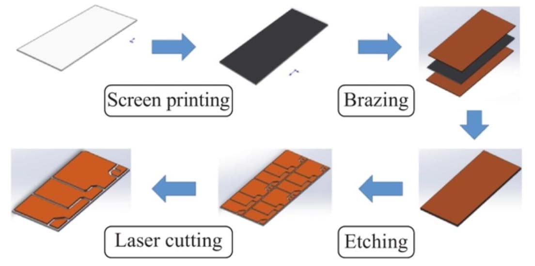
AMB ceramic PCB main technological process
The overall process flow of the ceramic copper substrate is as follows:
1. Surface treatment of the supplied copper and ceramics;
2. Stacking the copper and ceramics and putting them into a vacuum high-temperature furnace for welding;
3. Surface copper on the ceramic surface Chemical etching to generate designed patterns and lines;
4. Cutting the ceramic substrate with a laser and performing singulation to obtain a single core.
There are two main differences between DBC and AMB products:
1. The copper and ceramics of DBC products are directly bonded,
While the copper and ceramics of AMB products are brazed with active metal solder,
Which requires an additional silk screen process.
Before brazing, the active metal solder is evenly placed on the ceramic substrate;
2. The copper of the DBC product is formed by one etching,
While for the AMB product with an additional metal brazing layer,
An additional etching is required Process to remove solder, usually using hydrofluoric acid.
Taking AMB products as an example, the process flow of ceramic copper substrate is shown.
The main processes and materials will be introduced in detail below.

Why Choose AMB Ceramic PCBs?
1. High Thermal Conductivity
The AMB ceramic PCB has a thermal conductivity that is several times higher than traditional PCBs,
Making it an ideal choice for high-power applications.
This high thermal conductivity ensures efficient heat dissipation,
which is critical in preventing overheating and device failure.
PCB copper coins are used for heat dissipation at first.
The evolution of electronic devices and the emergence of tiny electronic circuits ,
It required a high heat dissipation solution with extended capacity in PCB.
2. High Frequency Operation
The AMB ceramic PCB has a low dielectric constant and loss,
Allowing it to operate at higher frequencies without signal distortion.
This makes it an ideal choice for high-frequency applications, such as RF and microwave circuits.
3. High Reliability
The AMB ceramic PCB is highly resistant to thermal shock,
Mechanical stress, and chemical corrosion.
It is an ideal choice for harsh environments and high-reliability applications,
Such as aerospace and automotive applications.

Applications of AMB Ceramic PCBs
The unique properties of AMB ceramic PCBs make them ideal for a wide range of high-performance electronic applications, including:
– Power Amplifiers
The high thermal conductivity of AMB ceramic PCBs makes them an ideal choice for power amplifier circuits.
This property allows the PCB to dissipate heat efficiently, reducing the risk of device failure due to overheating.
– LED Lighting
AMB ceramic PCBs are ideal for LED lighting applications as they can dissipate heat efficiently,
Preventing overheating of the LED chips.
The high reliability of these PCBs ensures that the LED lighting system remains functional for a long time.
– RF and Microwave Circuits
AMB ceramic PCBs have low dielectric loss and high-frequency operation,
Making them ideal for RF and microwave circuits.
These PCBs can transmit high-frequency signals without signal distortion, allowing for faster data transmission.
– Aerospace and Automotive Applications
The high reliability of AMB ceramic PCBs makes them an ideal choice for aerospace and automotive applications.
These applications require electronic components that can withstand harsh environments and high levels of stress.
– Conclusion
In conclusion, AMB ceramic PCBs are a significant innovation in the world of electronics.
Their high thermal conductivity, high-frequency operation,
And high reliability make them ideal for a wide range of high-performance electronic applications,
Including power amplifiers, LED lighting, RF and microwave circuits,
And aerospace and automotive applications.
As technology continues to advance,
AMB ceramic PCBs are expected to play an increasingly critical role in the development of high-performance electronics.
