
Heavy Copper PCB Design: Trace Width Calculation for High Current
Power electronics failures cause 35-50% of product returns in industrial and automotive applications, with undersized copper traces accounting for the majority. When standard 1-2 oz copper cannot handle current above 5-10A per trace, heavy copper PCB design becomes essential for motor drives, battery management systems, and high-power LED arrays.
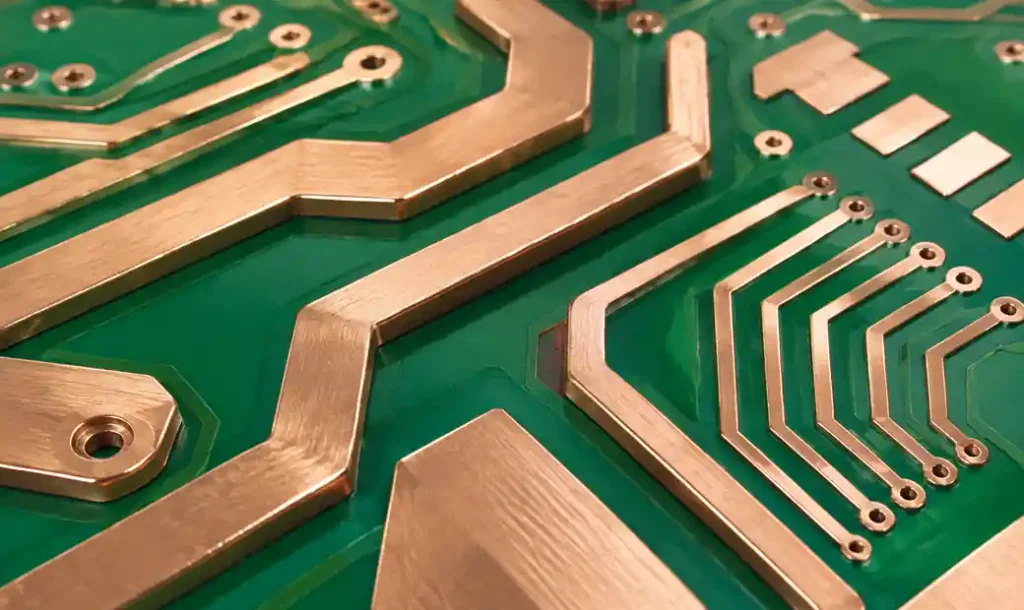
What is Heavy Copper PCB?
Heavy copper PCB features copper weights of 3 oz/ft² (105 μm) or greater, compared to standard 1 oz/ft² (35 μm). This increased thickness enhances current capacity, reduces resistive losses, and improves thermal dissipation. Per IPC-6012, heavy copper ranges from 3 oz to 10 oz, while extreme copper exceeds 10 oz up to 20 oz (700 μm). Manufacturing combines base copper foil with electroplating to balance cost with performance.
IPC-2221 Trace Width Calculation Formula
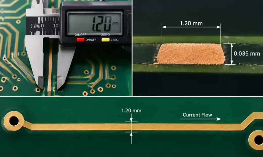
IPC-2221 provides trace width calculations based on allowable temperature rise:
Formula: Area [mil²] = (I / (k × ΔT^0.44))^(1/0.725), then Width = Area / (Thickness × 1.378)
Where k = 0.048 for external layers, k = 0.024 for internal layers, I is current in amperes, and ΔT is temperature rise above ambient in °C.
Example: A 10A trace with 1 oz copper and 10°C rise requires 181 mils (4.6 mm). With 4 oz copper, only 45 mils (1.14 mm)—a 75% reduction. This enables compact designs in power electronics PCB.
| Copper Weight | 5A Trace (10°C rise) | 10A Trace (10°C rise) | 20A Trace (10°C rise) | 30A Trace (10°C rise) |
|---|---|---|---|---|
| 1 oz (35 μm) | 90 mils (2.29 mm) | 181 mils (4.60 mm) | 362 mils (9.19 mm) | 543 mils (13.79 mm) |
| 2 oz (70 μm) | 45 mils (1.14 mm) | 90 mils (2.29 mm) | 181 mils (4.60 mm) | 271 mils (6.88 mm) |
| 4 oz (140 μm) | 23 mils (0.58 mm) | 45 mils (1.14 mm) | 90 mils (2.29 mm) | 136 mils (3.45 mm) |
| 6 oz (210 μm) | 15 mils (0.38 mm) | 30 mils (0.76 mm) | 60 mils (1.52 mm) | 90 mils (2.29 mm) |
Current Carrying Capacity vs Temperature Rise
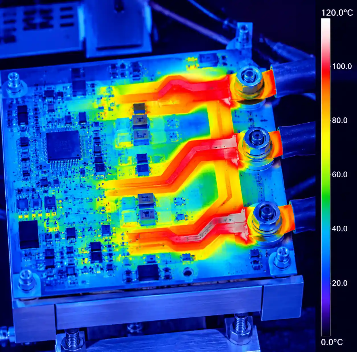
Temperature rise directly affects reliability. IPC-2221 allows 10°C rise for general applications, but conservative designs target 5°C for automotive and industrial equipment. Each 10°C increase reduces semiconductor lifespan by approximately 50% per Arrhenius equation, critical in BMS PCB design.
Power dissipation follows P = I² × R, where R = ρ × L / A. A 100 mm long, 10A trace in 1 oz copper (2.29 mm wide) has 1.06 mΩ resistance, dissipating 106 mW. In 4 oz copper, resistance drops to 0.27 mΩ, cutting power loss by 75% to 27 mW.
Ambient temperature compounds trace heating. At 85°C ambient with 10°C trace rise, total reaches 95°C—near the 105°C FR4 limit. High-Tg materials (170-180°C) become necessary when temperatures exceed 130°C, per PCB material properties.
Via Current Rating and Thermal Management
Plated through-hole vias transfer current between layers but create bottlenecks due to small cross-sectional area. A 12 mil (0.3 mm) via with 1 oz plating through 1.6 mm board has ~0.8 mΩ resistance—10-20× higher per unit length than traces.
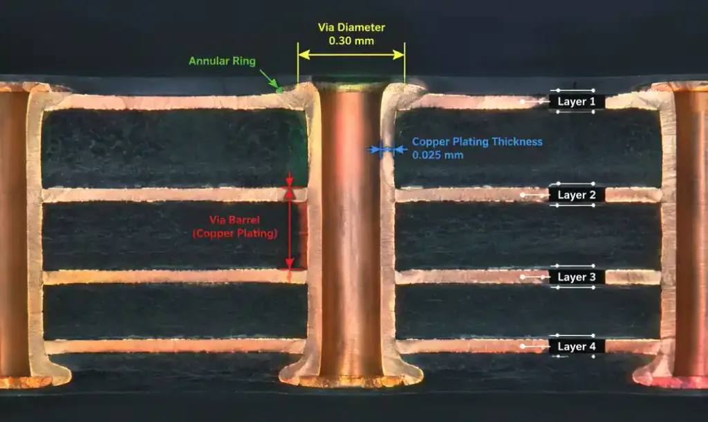
Current capacity scales with via barrel area: A = π × D × T × t. Multiple vias in parallel distribute current—four vias quadruple capacity. For 10A through a 4-layer board, use minimum 4× vias of 12-16 mil diameter.
Thermal vias enhance heat spreading from power components to planes. Via-in-pad designs require resin plugging to prevent solder wicking, ensuring reliable joints per IPC-7095. Space thermal vias 0.5-0.8 mm apart for optimal heat distribution in metal core PCB designs.
| Via Configuration | Diameter | Plating | Board Thickness | Resistance | Current Rating (10°C rise) |
|---|---|---|---|---|---|
| Single via | 12 mil (0.30 mm) | 1 oz | 1.6 mm (63 mil) | ~0.8 mΩ | 2.5-3A |
| Single via | 16 mil (0.41 mm) | 1 oz | 1.6 mm (63 mil) | ~0.6 mΩ | 3.5-4A |
| 4× parallel vias | 12 mil (0.30 mm) | 1 oz | 1.6 mm (63 mil) | ~0.2 mΩ | 10-12A |
| Single via | 20 mil (0.51 mm) | 2 oz | 2.4 mm (94 mil) | ~0.35 mΩ | 6-7A |
Heavy Copper Plating Process Considerations
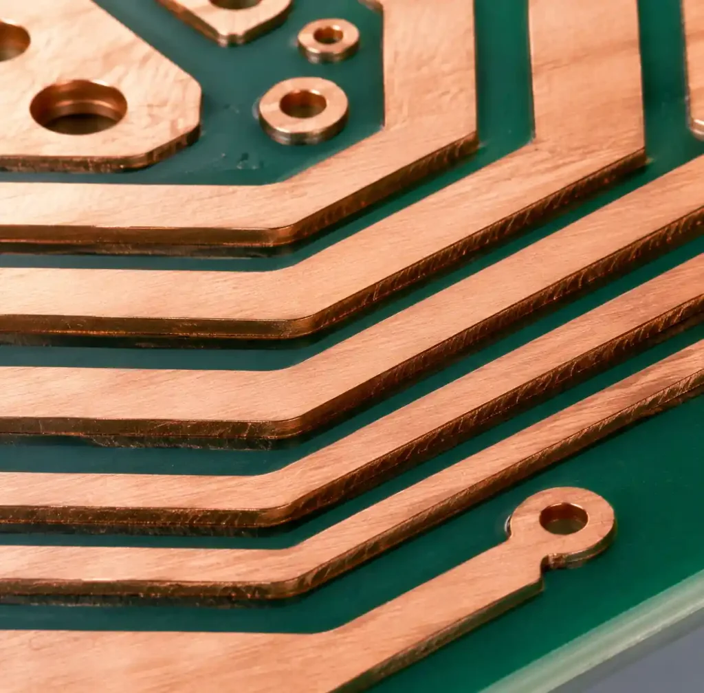
Manufacturing heavy copper requires extended electroplating that creates design challenges. Thicker copper increases sidewall undercutting during etching—for 6 oz copper, expect 3-4 mils (75-100 μm) undercut per side. Minimum trace width and spacing scale with copper weight: 4 oz requires 12/12 mils; 6 oz needs 15/15 mils. High aspect ratio holes (depth-to-diameter above 8:1) face plating challenges. Limit ratios to 6:1 for 4 oz copper, or use back-drilling in controlled impedance PCB designs.
Design Rules for Heavy Copper PCB
Proper design for manufacturing (DFM) prevents costly iterations. Key rules:
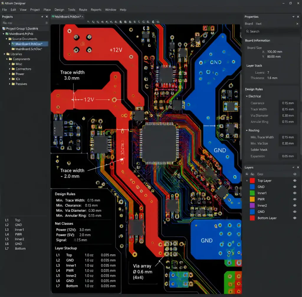
Trace width and spacing: Maintain minimum 15 mils (0.38 mm) for 6 oz copper. Use copper pours for return paths—a 10 mm pour has 1/10 the resistance of a 1 mm trace.
Corner radius: Sharp 90° corners concentrate current density. Use 45° chamfers or curved corners with radius ≥2× trace width, reducing current crowding by 30-40%.
Copper balancing: Distribute copper evenly across layers to prevent warpage. Add hatched pours on low-copper layers to reach 30-50% coverage. Unbalanced stacks warp 0.5-2 mm across 200 mm boards during lamination.
Annular ring: Provide minimum 8-10 mil ring for heavy copper. Standard 5 mil rings risk breakout during drilling with thick copper, per IPC-6012 tolerance.
Solder mask expansion: Increase opening by 3-4 mils beyond pad edges for thick copper, accounting for registration variation and edge roughness.
Thermal Modeling and Analysis
Finite element analysis (FEA) validates trace width calculations before prototyping. Modern PCB tools simulate conduction through copper and FR4, convection to air, and radiation losses. Input parameters include trace geometry, copper weight, current, ambient temperature, and boundary conditions.
Simulations show non-uniform temperature distribution—highest at trace center, dropping toward ends and vias. A 30A trace dissipating 2W may show 15°C rise at center but only 8°C at ends. Via stitching every 10-15 mm reduces peak temperature by connecting to internal planes.
For complex power networks, thermal-electrical co-simulation accounts for interactions: hot traces increase resistance (0.39%/°C), drawing more current from cooler paths. Designs should verify worst-case scenarios maintain safe temperatures.
Applications and Case Examples
Industrial motor drives: Three-phase inverters driving 5-15 kW motors require 30-50A per phase. Heavy copper boards use 6 oz copper, reducing 100 mm path resistance from 1.2 mΩ (2 oz) to 0.4 mΩ (6 oz). This cuts losses by 67%, saving 25-30W per board.
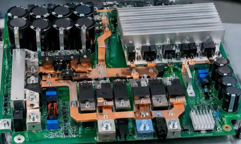
EV charging stations: Level 2 chargers (7.2 kW, 30A) use 4 oz copper for input rectification and 6 oz for DC output. Trace widths range from 80-120 mils with 5°C rise for -40°C to +65°C operation. Boards integrate conformal coating for outdoor protection.
High-power LED arrays: Architectural lighting panels (500W-1kW) use aluminum MCPCBs with 3-4 oz copper. Thermal vias connect through dielectric to aluminum base, maintaining junction temperature below 85°C for >50,000 hour lifespan.
Heavy Copper vs Standard Copper Trade-offs
Selecting between standard and heavy copper involves balancing performance, cost, and lead time. Standard 1-2 oz copper costs $50-150 for prototype 4-layer boards with 5-7 day lead time. Heavy copper (4 oz) increases price 40-80% and extends lead time to 10-15 days.
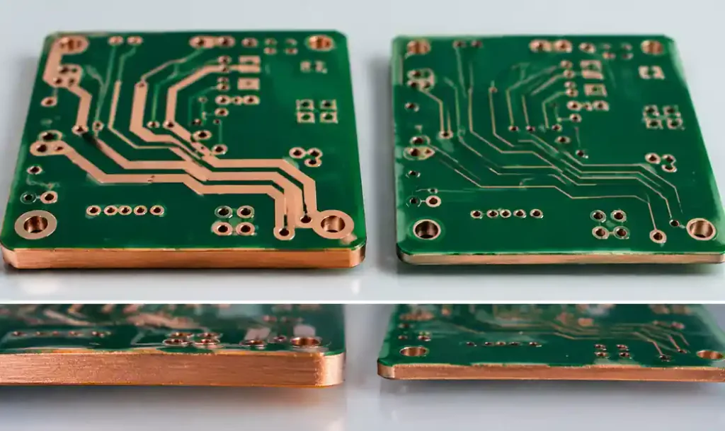
Cost scales non-linearly: 6 oz boards cost 2-3× standard pricing, while 10 oz extreme copper reaches 4-5×. Production runs above 100 pieces show smaller premiums (20-40%). Consider alternatives: wider traces in standard copper or MCPCB may meet requirements at lower cost.
Andwin Circuits offers heavy copper PCB manufacturing up to 10 oz with 7-10 day turnaround, supporting automotive and industrial applications with ISO 9001 and IATF 16949 certification.
| Parameter | Standard Copper (1-2 oz) | Heavy Copper (3-6 oz) | Extreme Copper (10-20 oz) |
|---|---|---|---|
| Current per trace | 1-10A | 10-50A | 50-200A |
| Min trace/space | 5/5 mil (0.13/0.13 mm) | 12/12 mil (0.30/0.30 mm) | 20/20 mil (0.51/0.51 mm) |
| Cost multiplier | 1× | 1.5-2.5× | 3-5× |
| Lead time | 5-7 days | 10-15 days | 15-25 days |
| Applications | General electronics, IoT | Motor drives, EV chargers | Arc welders, traction inverters |
FAQ
What copper weight should I specify for 15A continuous current?
For 15A with 10°C rise on external layers, 2 oz copper requires 120 mil (3.0 mm) width, 4 oz needs 60 mil (1.5 mm), and 6 oz uses 40 mil (1.0 mm). Internal layers need double the width. Specify 4 oz for compact designs. For high ambient (65-85°C), reduce rise to 5°C by doubling width or using 6 oz.
How do I calculate via count for high-current power planes?
Each standard via (12 mil diameter, 1 oz plating through 1.6 mm) carries ~2.5-3A with 10°C rise. For 15A, use minimum 5-6 vias in parallel, spaced 0.8-1.2 mm apart. For BGA power pins, use via-in-pad with resin plugging for better high-speed PCB performance.
Can I mix heavy copper layers with standard copper in one stackup?
Yes, hybrid stackups use heavy copper (3-6 oz) on outer layers for high-current traces and standard copper (1-2 oz) on inner layers for signals. This reduces cost while providing current capacity where needed. Specify copper weight per layer in fabrication notes.
What is the temperature coefficient of copper resistance?
Copper resistance increases 0.39% per °C. A trace with 1 mΩ at 25°C reaches 1.26 mΩ at 85°C—a 26% increase. This creates positive feedback. Design with 25-30% resistance margin and verify with thermal simulation.
Do I need thermal relief for power plane connections?
Avoid thermal relief for power paths above 5A—use solid connections to minimize resistance. This requires higher soldering power (80-120W) for PCB assembly. Signal pads can use standard 4-spoke relief for ease of rework.
Conclusion
Heavy copper PCB design balances electrical performance, thermal management, and manufacturing constraints. IPC-2221 provides trace width baselines, but real designs must account for via distribution, plating limitations, and copper balancing.
For current above 10A per trace, 4-6 oz heavy copper reduces board size, lowers resistive losses, and improves thermal spreading. Hybrid stackups mixing heavy outer layers with standard inner layers optimize cost while meeting requirements.
Andwin Circuits specializes in heavy copper PCB manufacturing from 3 oz to 10 oz with 7-10 day delivery. ISO 9001 and IATF 16949 certified for automotive, industrial control, and power electronics. We provide DFM review and turnkey PCB assembly.
Contact us today for custom heavy copper PCB solutions and factory-direct pricing.