
Via in Pad Design Rules: Plugging, Tenting, and Capping Methods
Via in pad design accounts for 15-25% of surface mount assembly yield issues when improperly specified. IPC-4761 testing shows unfilled or poorly finished vias cause solder wicking, voiding, and component tilt failures in up to 30% of BGA assemblies.
If you want to design reliable via in pad connections for BGAs, QFNs, or thermal management applications, then you need to understand three primary via finishing methods: resin plugging, soldermask tenting, and copper capping. Each method offers distinct advantages for flatness, cost, thermal performance, and assembly reliability.

What is Via in Pad Design?
Via in pad places a plated through-hole via directly underneath a surface mount pad rather than offsetting it. This technique saves board space, shortens signal paths, and improves thermal conductivity by creating a direct thermal path from component to inner copper layers.
The challenge is that open or inadequately finished vias create reliability problems during assembly. Solder paste flows into the via barrel during reflow, causing solder joint voiding (15-40% volume reduction), insufficient fillet height, and poor component coplanarity. IPC-A-610 Class 3 requires less than 25% voiding for high-reliability applications.
You can use via in pad for BGA packages with fine pitch (≤0.8mm), QFN thermal pads, high-power components requiring thermal vias, and HDI designs where routing density demands maximum space efficiency.
Via Finishing Methods Comparison
| Method | Flatness | Cost | Thermal | Best For |
|—|—|—|—|
| Soldermask Tenting | Fair (±50μm) | Lowest | Poor | Prototypes, ≥1.0mm pitch |
| Resin Plugging | Excellent (±25μm) | Moderate | Good | Fine-pitch BGA, Class 3 |
| Copper Capping (VIPPO) | Excellent (±15μm) | High | Excellent | Thermal vias, power |
| Conductive Fill | Excellent (±20μm) | Highest | Excellent | High-current, RF signals |
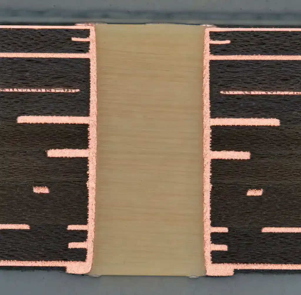
Via Plugging with Resin: Non-Conductive Fill
Via plugging fills the via barrel with non-conductive epoxy resin, then planarizes the surface flush with the copper pad. The standard process uses vacuum-assisted resin injection to eliminate voids, followed by planarization to achieve flatness within ±25μm. IPC-4761 Type VII specifies this construction.
Plugged vias support fine-pitch BGAs down to 0.4mm pitch and reduce solder joint voiding to under 10%. Thermal conductivity is moderate because the non-conductive epoxy blocks direct heat transfer.
Specify resin plugging for HDI PCBs with BGA packages, medical and automotive applications requiring IPC-6012 Class 3.
Design Rules for Resin-Plugged Vias
Finished via diameter: 0.25-0.5mm for reliable plugging. Minimum pad annular ring: 0.1mm beyond via diameter. Via depth: maximum 10:1 aspect ratio for complete fill. Pad size: via diameter + 0.2mm minimum. Space plugged vias at least 0.5mm apart under single BGA pads.
Soldermask Tenting: Low-Cost Via Covering
Soldermask tenting covers the via opening with soldermask without filling the barrel. This is the most economical solution but offers limited reliability for fine-pitch applications.
The tented soldermask forms a thin membrane (15-30μm) over the via opening. During reflow, pressure and heat can rupture the mask, allowing solder to wick into the barrel and create voiding.
Tenting works for via diameters up to 0.3mm. Thermal performance is poor because the air-filled via barrel blocks heat transfer. Use for prototypes, low-volume production, and designs with pad pitch ≥1.0mm. Do not specify for IPC Class 3 or fine-pitch BGAs.
Tenting Design Constraints
Maximum via diameter: 0.3mm for reliable tenting. Pad pitch: ≥1.0mm recommended. Heavier components (>5g) and multiple reflow cycles increase rupture risk. Include “soldermask tenting per IPC-SM-840” in fabrication notes.
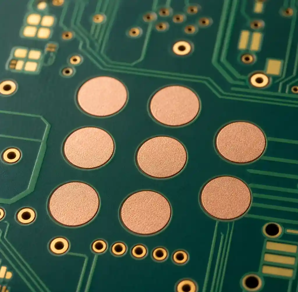
Via Capping Methods: Epoxy and Copper Plating
Via capping fills the via with resin, then deposits a conductive copper layer over the plug to create a solderable, thermally conductive surface. This premium method combines the flatness of plugging with excellent thermal and electrical performance.
Epoxy Capping (VIPPO)
Epoxy capping plates 15-25μm of copper over a resin-plugged via, creating a fully planar surface with superior thermal conductivity. The process: drill and plate vias, plug with epoxy, planarize, apply copper, pattern outer layers.
Epoxy-capped vias achieve ±15μm flatness, support 0.3mm pitch BGAs, and reduce thermal resistance by 40-60% compared to non-conductive plugs. The copper cap also provides electromagnetic shielding for RF designs.
Specify epoxy capping for power components with thermal vias, RF designs requiring grounded vias, and applications where thermal cycling demands maximum reliability.
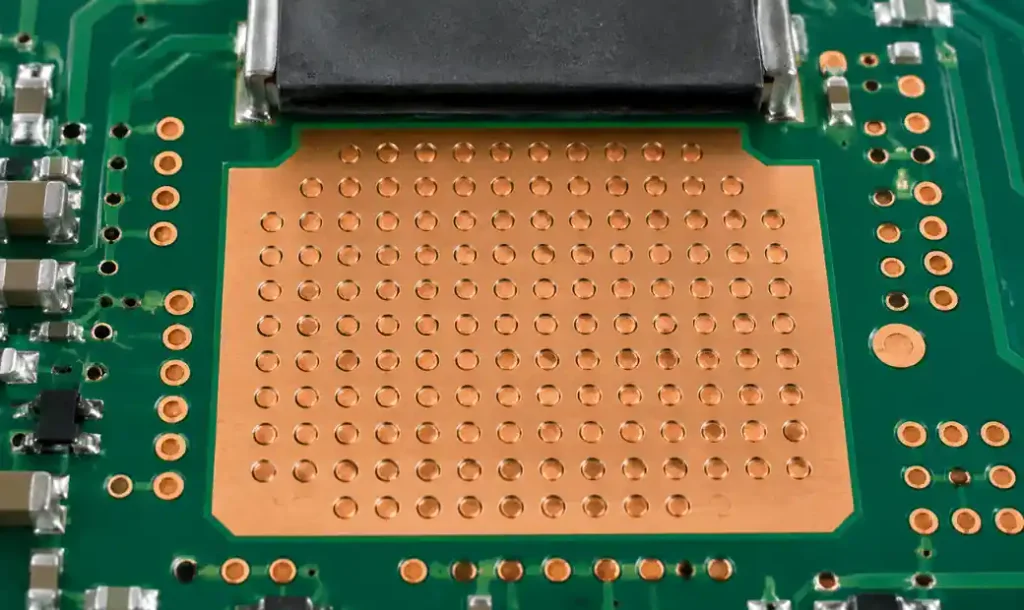
Copper-Filled Vias (Conductive Fill)
Copper-filled vias use electroplated or conductive paste to completely fill the via barrel with conductive material. This offers the best thermal and electrical performance.
Fully copper-filled vias reduce thermal resistance by 70-80%, support high current density (50-100A/mm²), and provide superior signal integrity for high-speed differential pairs.
Specify copper filling for thermal management critical designs, high-current metal core PCBs, and ultra-high-speed signals (≥25Gbps).
Cost Comparison and Selection Criteria
Via finishing cost varies significantly based on method, via count, and manufacturer capability.
Soldermask tenting adds $0-5 per board. Resin plugging adds $15-40 per board depending on via count. Epoxy capping (VIPPO) adds $25-60 per board. Copper filling adds $40-100 per board for specialized plating.
Lead time increases 2-3 days for plugging, 3-5 days for capping, and 5-7 days for copper filling. Quick turn services may not offer premium via finishing in expedited timeframes.
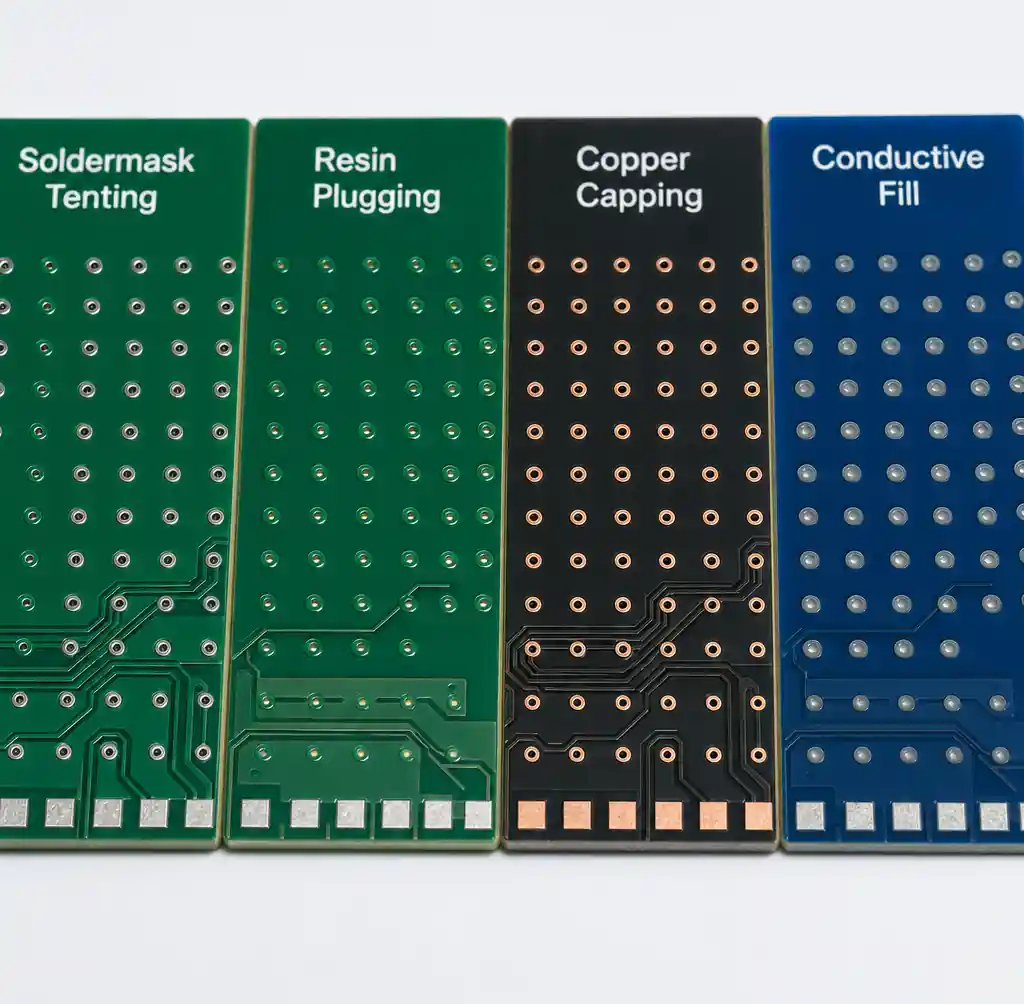
Selection Decision Matrix
Choose soldermask tenting when: prototype or low-volume (≤100 units), pad pitch ≥1.0mm, via diameter ≤0.3mm, IPC Class 1-2, cost is primary constraint.
Choose resin plugging when: fine-pitch BGA (0.4-0.8mm), IPC Class 3 reliability required, production volume ≥500 units, moderate thermal performance acceptable.
Choose epoxy capping when: thermal vias under power components, thermal resistance reduction of 40-60% needed, EMI shielding required under RF components.
Choose copper filling when: maximum thermal performance required (≥70% improvement), high current density (≥50A/mm²), ultra-high-speed signals (≥25Gbps).
Design Guidelines for BGA Via in Pad
BGA packages drive most via in pad applications because fine pitch and high pin counts demand maximum routing density.
Via Sizing and Placement
Via finished diameter: 0.25-0.35mm for 0.5-1.0mm pitch BGAs. Smaller vias (0.20-0.25mm) suit 0.4mm pitch, larger vias (0.35-0.50mm) work for ≥1.0mm pitch. Via barrel must be plated to minimum 25μm copper thickness.
Center vias under BGA pads to maximize thermal transfer. For large thermal pads, use via arrays (2×2 or 3×3) with 0.5-0.8mm spacing.
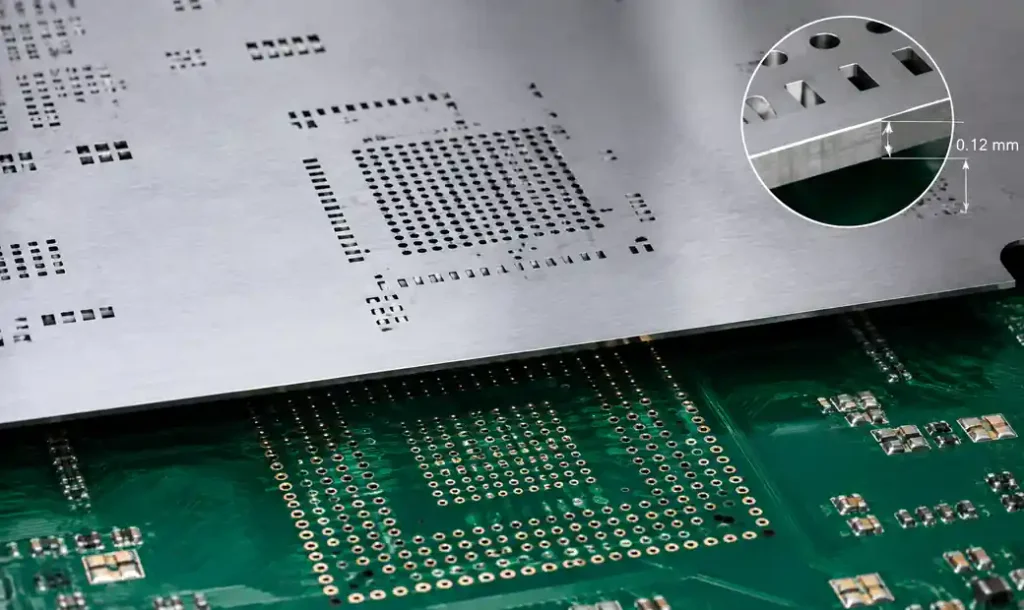
Stencil Aperture Design
Reduce stencil aperture size by 10-20% for plugged via pads. For 0.5mm BGA pad with 0.3mm plugged via, use 0.40-0.45mm aperture to prevent excess solder paste and reduce voiding.
Stencil thickness: 0.10-0.125mm for fine-pitch BGAs. Specify nano-coated or electropolished stencils to improve paste release over plugged vias.
Thermal Via Design for Power Components
Thermal vias provide the primary heat escape path for power components, making via design critical for junction temperature and long-term reliability.
Thermal Via Array Configuration
For standard 0.3mm thermal vias, thermal resistance is approximately 70°C/W per via. A 3×3 array (9 vias) achieves ~8°C/W thermal resistance, adequate for 1-3W components.
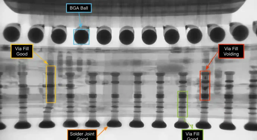
Space thermal vias 0.8-1.2mm center-to-center. Connect via arrays to continuous copper pours on inner layers. Minimum copper pour area is 4x the component thermal pad area.
| Via Type | Thermal Resistance (°C/W) | Cost | Power Range |
|---|---|---|---|
| Resin Plugged | 70-90 | 1.5x | <1W |
| Epoxy Capped | 40-60 | 2.5x | 1-3W |
| Copper Filled (Paste) | 25-35 | 3.0x | 3-5W |
| Copper Filled (Plated) | 15-25 | 4.0x | >5W |
Common Via in Pad Failures and Prevention
Understanding failure modes helps you specify appropriate via finishing methods and design rules.
Solder Joint Voiding
Voids form when solder wicks into incompletely plugged vias during reflow, leaving air pockets. Voiding reduces joint strength by 40-60% when void area exceeds 25% of pad area.
Prevention: specify IPC-4761 Type VII with void content ≤5%, reduce stencil aperture by 10-15% over plugged vias, use vacuum reflow when voiding consistently exceeds 15%.
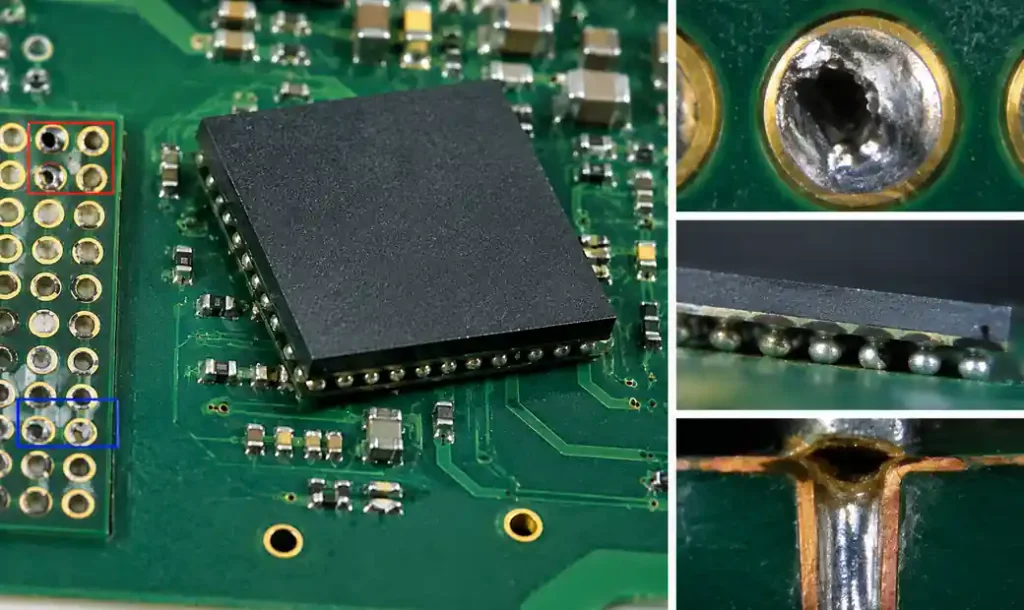
Component Tilt and Coplanarity Issues
Uneven via plug flatness causes component tilt during reflow. BGA tilt exceeding 0.1mm results in 15-30% joint failure rate on fine-pitch packages.
Prevention: specify via flatness tolerance ±25μm or tighter, use uniform via finishing method across all pads under a component, verify flatness with white light interferometry before assembly.
Thermal Performance Degradation
Non-conductive via plugs increase thermal resistance by 40-70% compared to capped vias, causing junction temperature increase and reduced component lifespan.
Prevention: specify copper-filled or epoxy-capped vias for thermal-critical designs, use thermal simulation to verify via array sizing, measure junction temperature on first articles to validate performance.
Frequently Asked Questions
What is the difference between via plugging and via capping?
Via plugging fills the via with non-conductive epoxy resin and planarizes the surface. Via capping adds a conductive copper layer over the resin plug, creating better thermal and electrical performance. Capping costs 50-80% more but reduces thermal resistance by 40-60%.
Can I use soldermask tenting for BGA packages?
Soldermask tenting works for larger pitch BGAs (≥1.0mm) with via diameter ≤0.3mm on IPC Class 1-2 products. Fine-pitch BGAs (≤0.8mm) require resin plugging because tenting rupture rates exceed 10-20% during assembly.
How much does via in pad cost compared to via offset designs?
Resin plugging adds $15-40 per board for typical designs with 20-50 vias. Offsetting vias eliminates this cost but requires 15-30% more board area, increasing base fabrication cost by $5-15 per board.
What is IPC-4761 Type VII specification?
IPC-4761 Type VII specifies vias filled with non-conductive material and planarized to create a flat, solderable surface. It requires complete fill with ≤5% void content and surface flatness within ±25μm for Class 3 products.
How many thermal vias do I need under a QFN thermal pad?
For standard 0.3mm vias, use 4-6 vias for 1W components, 9-12 vias for 2-3W components, and 16+ vias for >5W components. Each 0.3mm thermal via contributes approximately 70°C/W thermal resistance.
Does via in pad affect signal integrity on high-speed designs?
Resin-plugged vias create impedance discontinuity of 3-8 ohms on controlled impedance traces, acceptable for signals <10Gbps. For ≥25Gbps signals, specify copper-filled vias to minimize inductance.
Conclusion
Via in pad design rules determine assembly reliability, thermal performance, and manufacturing cost for high-density PCBs. Soldermask tenting offers the lowest cost for prototypes but lacks reliability for fine-pitch BGAs. Resin plugging provides excellent flatness for production volumes above 500 units. Epoxy capping and copper filling deliver superior thermal performance for power components at premium cost.
If you need HDI PCB manufacturing with professional via in pad finishing, Andwin Circuits offers IPC-4761 certified resin plugging, copper capping, and conductive fill up to 50 layers. Our advanced capability includes ±15μm flatness tolerance, 0.2mm minimum via diameter, and complete void control for IPC Class 3 automotive and medical applications.
Contact us today for via in pad design support, capability specifications, and competitive factory-direct pricing for your next PCB project.