Ceramic PCB manufacturer
in China
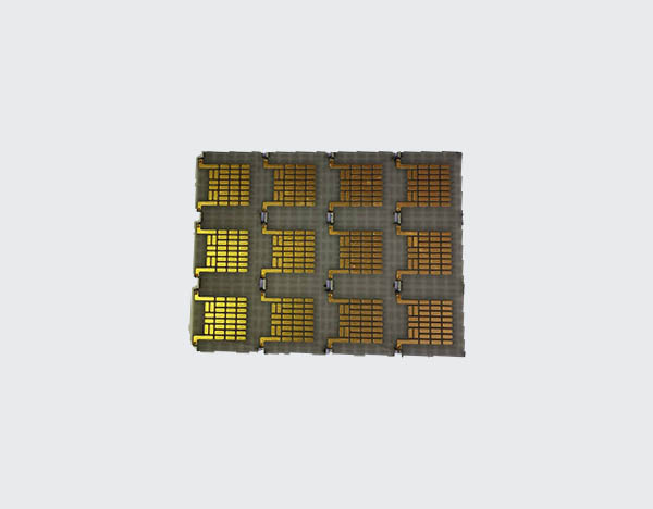
Ceramic PCB Fab. from 1 to 12 layers
Alumina | Aluminum nitride | Silicon nitride | Beryllium Oxide |
Boron Nitride | Silicon Carbide (SiC) | Zirconia ( ZrO2 ) |
We provide many types Ceramic PCB with special requirement.
Min. trace W / S : 25/25um, Max. Copper thickness: 800um
Cermaic PCB manufacturer worth trusted
Andwin PCB provide Ceramic PCB manufacturing since 2010,
Our ceramic PCB material include Alumina(Al2O3), Aluminum nitride(AIN ALN), Silicon nitride (SIN), Beryllium Oxide (BeO), Boron Nitride (BN), Silicon Carbide (SiC) ,Zirconia ( ZrO2 ) etc.
The ceramic PCB manufacturing technical use DPC, DBC, Thick film and AMB.
Andwin have strongly ceramic PCB manufacturing capability to match your requirement.
Our team’s strongly ceramic PCB experience and on time delivery capacity help MicroSoft , FaceBook’S VR/AR project to enter market 2 years earlier than expect time!
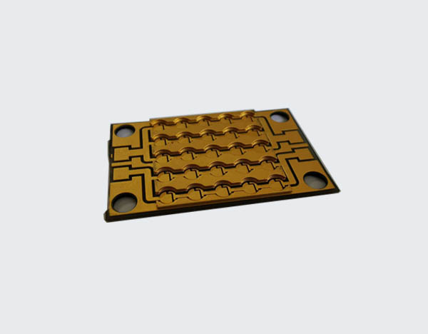
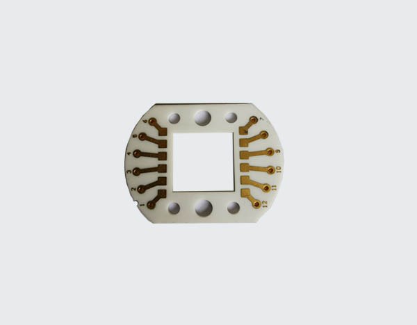
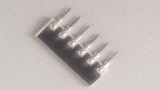
Material: Al2O3 ( Alumina )
Technical: DPC (Direct plate copper )
Plate copper edge side
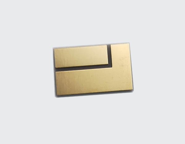
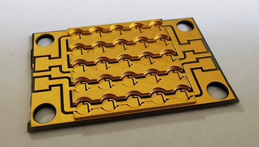
Material: Al2O3 ( Alumina )
Technical: DBC (Direct Bond copper )
Copper Thickness 300um
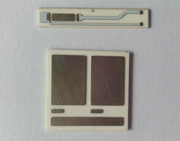
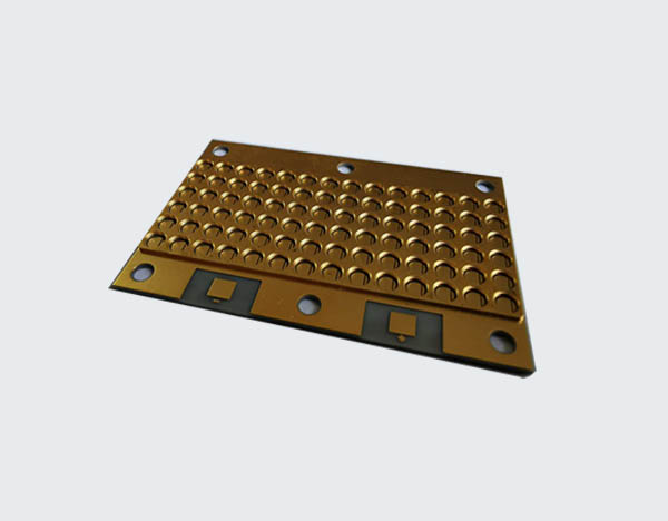
Material: AIN
( Aluminum nitride )
Technical: DPC
Supper smooth( Sand blast )
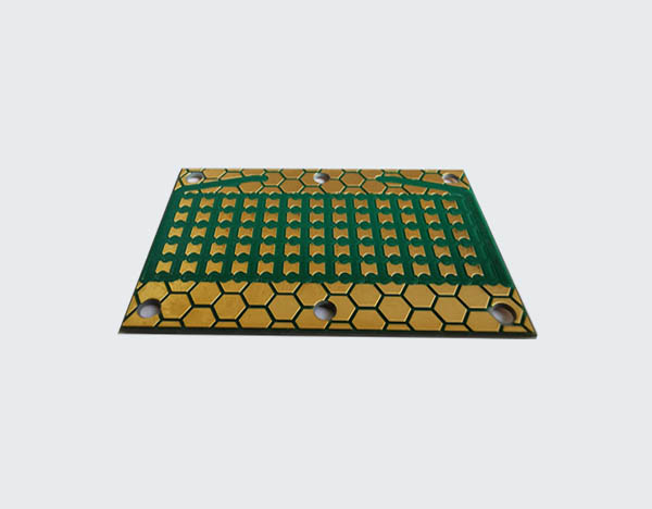
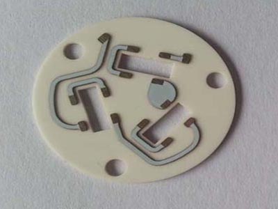
Material: Al2O3( Alumina )
Technical: Thick film
Printed resistor
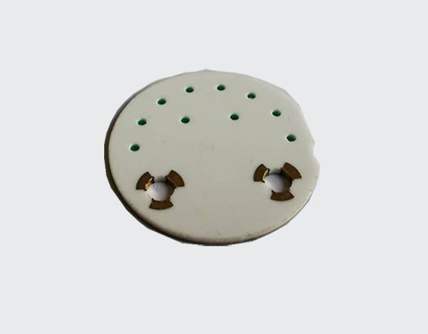
Material: Zirconia ( ZrO2 )
Technical: DPC
Zirconia substrate 7.0mm
Material: Silicon nitride
Technical: AMB
SIN 0.32mm Copper 0.3mm
Why choose us?
Free DRC – Design Rule Check
Our engineer 100% DRC your Gerber file before manufacturing.
100% E-Test – All FPC are tested,this process could ensure all FPC are
work well.
Visual – FQC FQA
Our engineer 100% visual your final FPC.
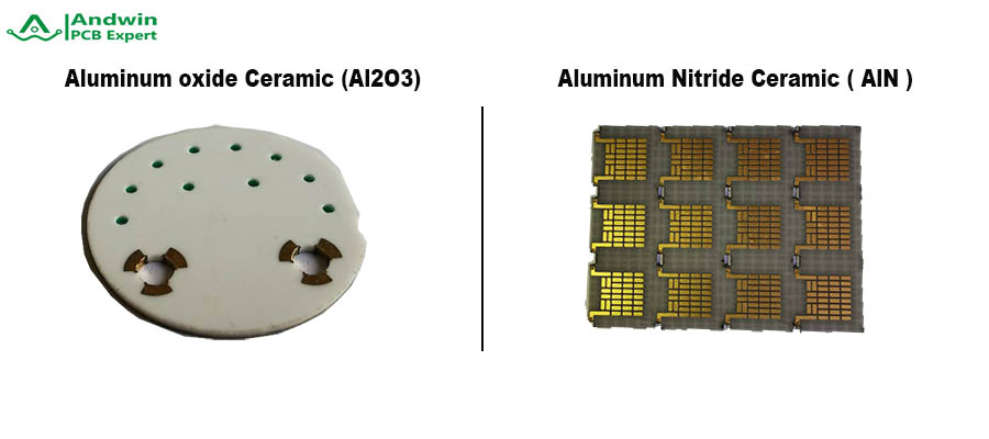
Aluminum oxide ( Al2O3 ) Ceramic PCB
Aluminum oxide Ceramic PCB substrate (Al2O3) is white color
Thermal conductivity Min. 24 W/m.k up to 30W/m.k
Aluminum Nitride (AIN / ALN) Ceramic PCB
Aluminum Nitride Ceramic PCB substrate ( AlN ) is brown
Thermal conductivity Min.275 W/m.k up to 320 W/m.k

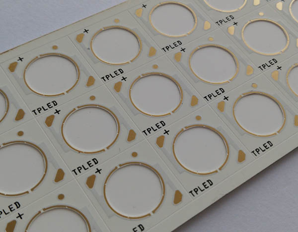
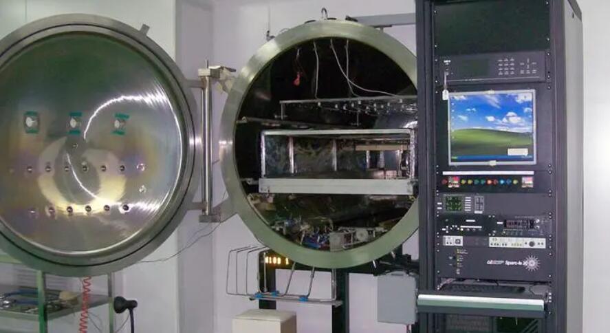
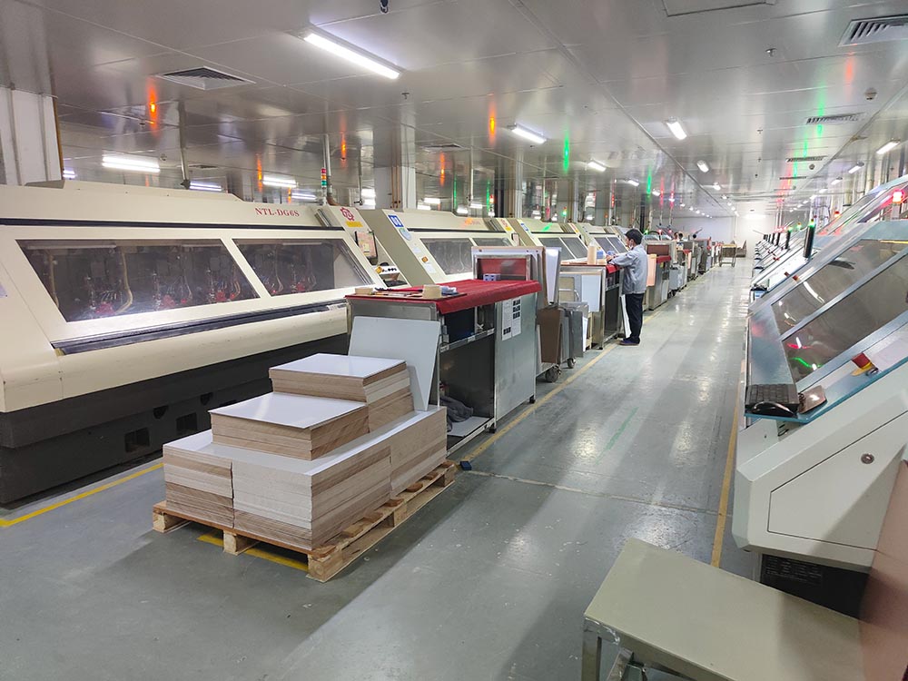
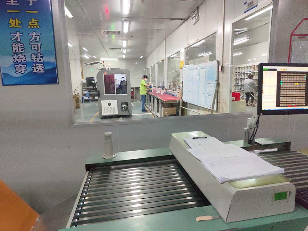
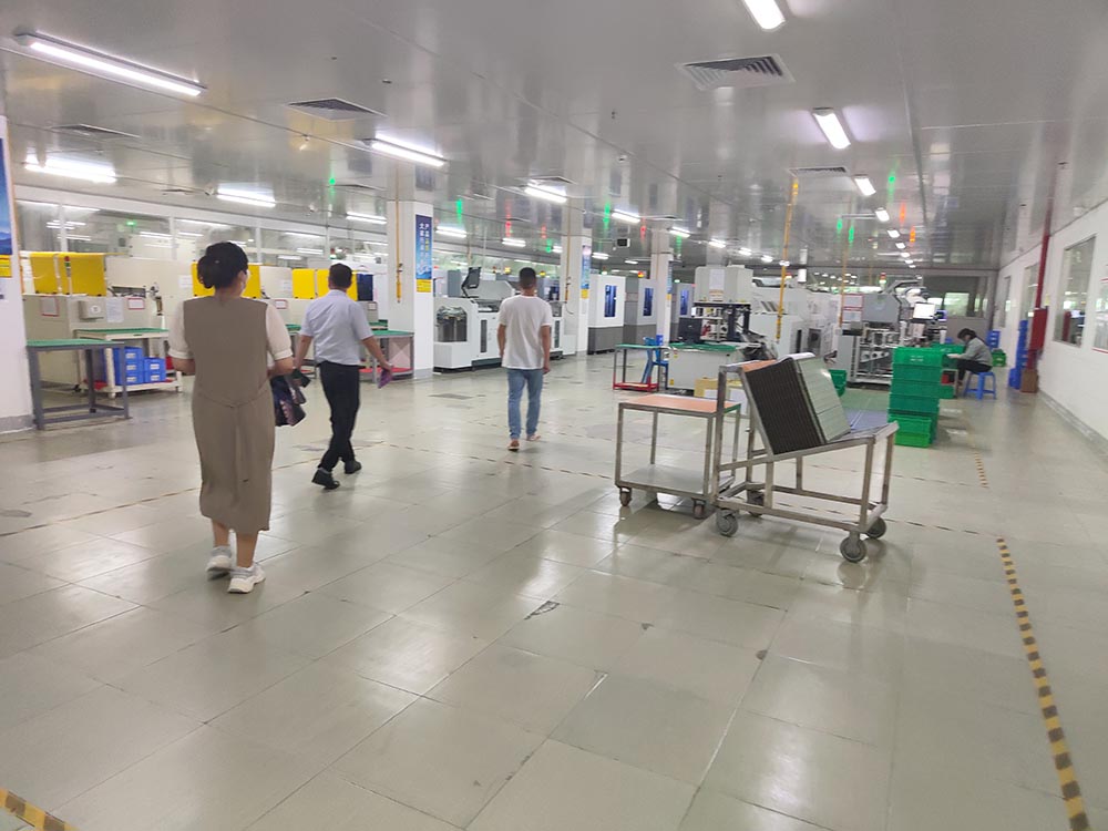
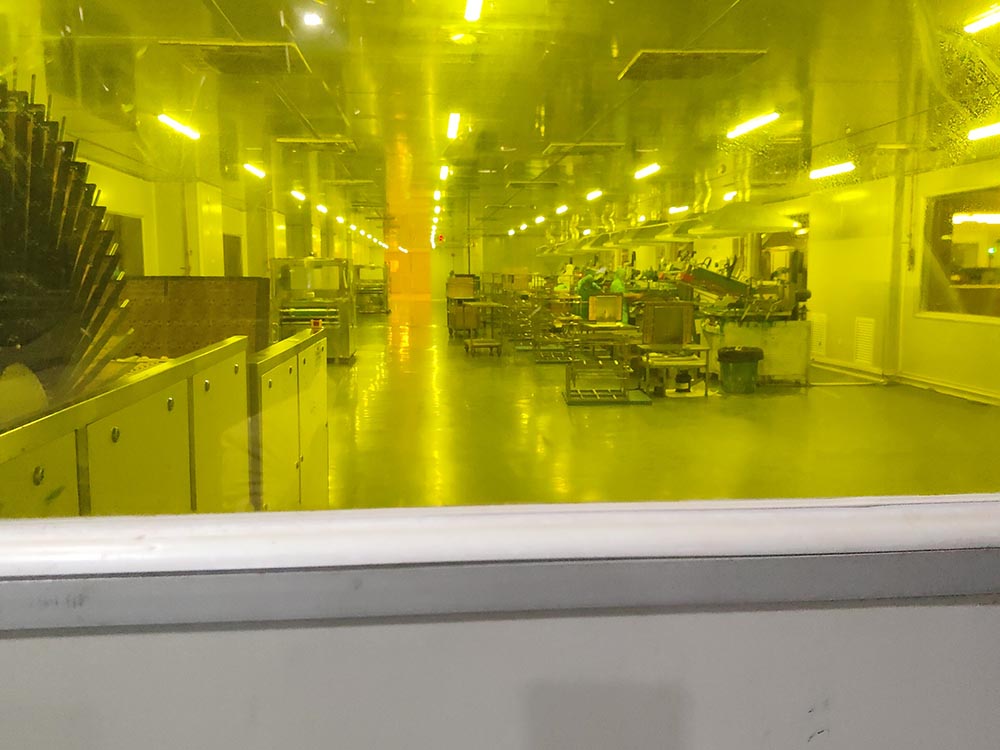
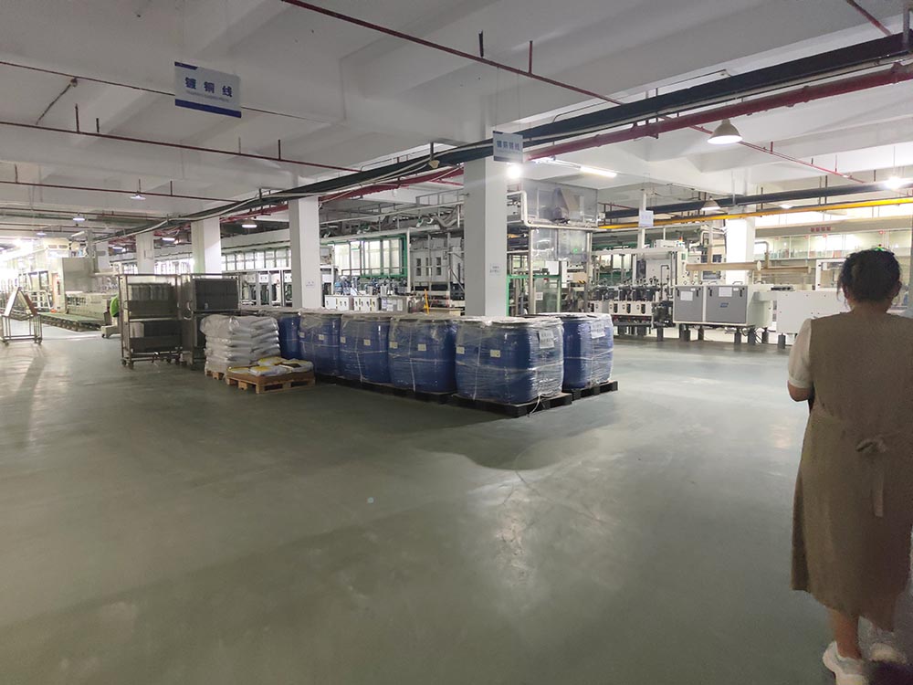
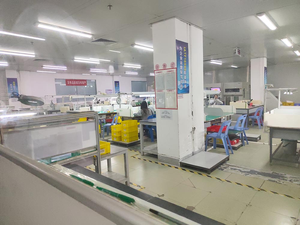
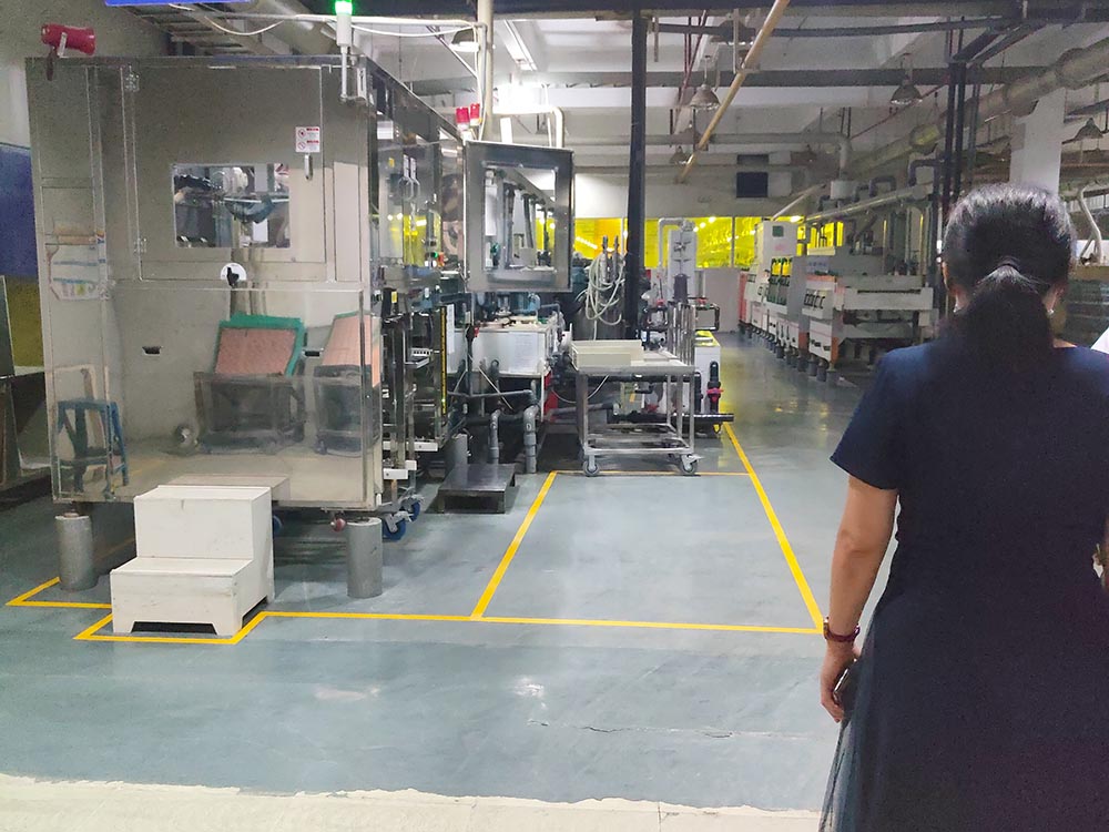
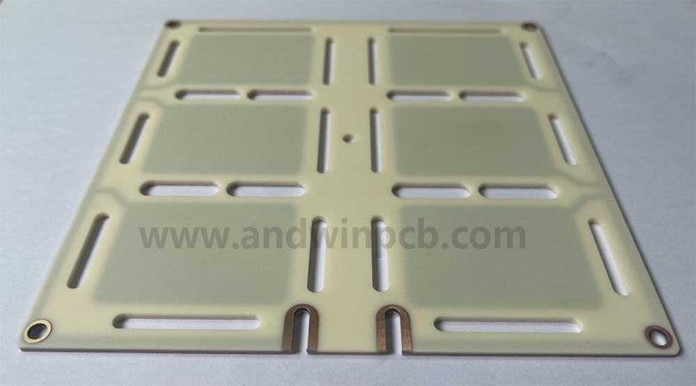
Factory show
Which industral we serviced?
High Power LED lighting

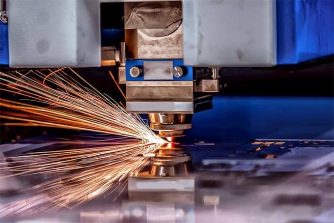
Laser machine Application:
Medical Equipment :

Aeronautics and space :

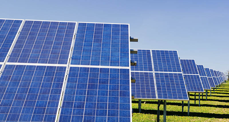
Solar energy :
Ceramic PCB widely be use in many industries,
Please contact us by e-mail : sales@andwinpcb.com for you ceramic PCB
Ceramic PCB manufacturing Capability
| Andwin ceramic PCB Technical Capability | |||
| Item | Standard | Minimum(mm) | Maximum (mm) |
| Board thickness | 0.635/0.8/1.0mm | 0.12mm | 7.0mm |
| Material | Aluminum nitride Aluminum oxide Zirconium oxide Carborundum | / | / |
| Layer count | 1 – 12 Layers | / | / |
| Drilling | 0.1mm | 0.075mm( 3 mil ) | |
| Drilling Tolerance | +/-0.03mm | / | / |
| Drill/Thick aspect rate | 1:8 | 1:10 | / |
| DBC Copper thickness | 0.3mm ( 10 oz ) | 100um ( 3 OZ ) | 525um ( 15 OZ) |
| DPC Copper thickness | 18.5um ( 0.5 oz) | 5um | 105um(3 OZ) |
| Lines Width | 120um ( 5 mil ) | 25um( 1mil ) | / |
| Lines spaces | 120um ( 5 mil ) | 25um( 1mil ) | |
| Final surface finishing | ENIG | / | / |
| ENIPIG | / | / | |
| Immersion Silver | / | / | |
| Immersion Tin | / | / | |
| OSP | / | / | |
More knowleage about ceramic PCB
What is ceramic PCB?
Ceramic PCB (Printed Circuit Board) is a type of circuit board made of ceramic materials
such as alumina,aluminum nitride, Silicon nitride (SI3N4),Beryllium Oxide,Boron Nitride,
Silicon Carbide and Zirconia etc.

These materials have high thermal conductivity and excellent electrical insulation properties,
Making them suitable for high-power and high-frequency applications.
Ceramic PCBs are commonly used in electronic devices such as laser device, power modules,
LED lighting, and microwave devices.
They are also known for their durability, reliability, and resistance to thermal and mechanical stress.
Due to ceramic PCBs have high thermal conductivity and low expansion coefficient (CTE),
Ceramic circuit boards are more versatile, less complex and offer superior performance
Compared to regular PCBs.
Many users of printed circuit boards find ceramic PCBs have an advantage over traditional boards made of other materials.
How many types ceramic PCBs?
- DPC ceramic PCB
- DBC ceramic PCB
- Thick film ceramic circuit board
- AMB ceramic circuit board
1. DPC ceramic PCB
DPC is direct plate copper technical.
DPC ceramic PCB stands for Direct Plated Copper ceramic Printed Circuit Board.
It is a type of printed circuit board that uses a ceramic substrate instead of a traditional fiberglass substrate (FR4).
The ceramic material offers better thermal conductivity and electrical insulation properties,making it ideal for high-power and high-frequency applications.
The DPC technology involves directly plating copper onto the ceramic substrate,
eliminating the need for a separate copper layer,
which reduces the board’s thickness and improves its thermal performance.
DPC ceramic PCBs are commonly used in power electronics, LED lighting, and aerospace applications.

DPC ceramic PCB advantage:
1. Min. conductor thickness: 10um (0.4mil )
The mean, You could design line width and space with very small
Min. Line width/Space :10um/10 um ( 0.4 / 0.4 mil )
2. More ceramic PCB substrate options
- Alumina ( AL2O3 96% 99.6% )
- Aluminum nitride (AIN ALN )
- Silicon nitride ( SI3N4 )
- Beryllium Oxide ( BeO )
- Boron Nitride ( BN )
- Silicon Carbide (SiC)
- Zirconia ( ZrO2 )
Andwin could meet all of your DPC ceramic PCB substrate requirement,
You could choose suitable Ceramic PCB substrate for your electronic products.
DPC ceramic PCB Shortcoming:
Also,DPC ceramic PCB could meet your heavy copper upto 300um,
But the cost is very high.
Andwin provide you a economical suggestion – DBC ceramic PCB.
2. DBC ceramic PCB
DBC is direct bond copper technique.

Copper foil bonded directly to alumina (AL2O3) or aluminum nitride (AIN,ALN) substrates one sided or double side at high temperatures.
Copper thickness: Min. 70um ( 2 OZ ) upto 300um
Ceramic material: alumina (AL2O3) or Aluminum nitride(AIN,ALN)
DBC Ceramic PCB advantage:
Meet thick copper requirement with comfortable cost,
Widely use IGBT and solar energy
DBC ceramic PCB Shortcoming:
Could not do plate through holes ( PTH )
3. Thick film ceramic PCB
Thick film ceramic printed circuit board is a type of ceramic PCB
That uses a thick film deposition process to create conductive traces and other circuit elements
on the ceramic substrate.

The thick film deposition process involves printing a paste of conductive materials, such as silver, gold, or platinum, onto the surface of the ceramic PCB substrate.
And then firing it at high temperatures to create a permanent bond between the conductive material and the ceramic substrate.
This process is repeated to create multiple layers of conductive traces and insulating layers,resulting in a multi-layered ceramic PCB.
Thick film ceramic PCBs are commonly used in high-temperature and high-power applications,
Such as power electronics, automotive electronics, and aerospace industries,
Due to their excellent thermal conductivity and high mechanical strength.
Thick film ceramic PCB advantage:
1.It is lower cost ceramic PCB if use silver conductor
2.Via holes avaible for double sided ceramic circuit board.
Thick film ceramic PCB shortcoming:
Min.conductor width/Space : 0.15mm/0.15mm
During the thick film ceramic circuit board use silk printed technique,
Could not do very thin trace.
4. AMB ceramic circuit board
AMB is active metal brazing technology.
The AMB ceramic PCB is a type of printed circuit board that uses a ceramic PCB substrate instead of the traditional fiberglass or epoxy substrate.
AMB technology is a further development of DBC technology.
It is a method of combining ceramics and metals by using active metal elements (such as Ti/Ag/Zr/Cu) in solder.
Ceramics form a reactive layer that can be wetted by liquid solder.
The bonding in the AMB ceramic substrate is achieved by the chemical reaction of the ceramic and the active metal solder at temperature,
And the Si3N4 ceramic used in the AMB has a higher thermal conductivity (>90W/mK) Compared to the traditional Al2O3 ceramic substrate 25°C),
Which is closer to the thermal expansion coefficient of silicon (2.6×10 -6 /K).
Therefore, the AMB substrate has high adhesive strength and reliability.
Combined with silver sintering process and high-power silicon carbide chip,
AMB copper layer with active metal coating can realize high power,
Better heat dissipation and high reliability packaging module (can withstand 3000 thermal shocks),
Which has been widely used in Electric vehicles,electric motives and high-speed trains.

How to choose your ceramic pcb substrate material?
alumina,aluminum nitride, Silicon nitride (SI3N4),Beryllium Oxide,Boron Nitride,
Silicon Carbide and Zirconia
There are 2 types ceramic pcb substrate material are widely be used,
Aluminum oxide Ceramic (Al2O3) and Aluminum Nitride Ceramic ( AlN )
Also, there are called as aluminum oxide Ceramic pcb or Aluminum Nitride Ceramic pcb.
Aluminum oxide Ceramic PCB substrate (Al2O3) is white color
Thermal conductivity Min. 24 W/m.k up to 30W/m.k
Aluminum Nitride Ceramic PCB substrate ( AlN ) is brown
Thermal conductivity Min.275 W/m.k up to 320 W/m.k
Silicon nitride
Thermal conductivity Min.20 w/m.k upto 80 w/m.k
Beryllium Oxide ( BeO )
Thermal conductivity Min.200 w/m.k upto 250 w/m.k
Boron Nitride ( BN )
Thermal conductivity Min.80 w/m.k upto 600 w/m.k
Silicon Carbide (SiC)
Thermal conductivity Min.80 w/m.k upto 180 w/m.k
Zirconia ( ZrO2 )
Thermal conductivity 5 – 20 W/m.k
At room temperature (25°C), the thermal conductivity of zirconia is about 5-8 W/(m·K).
When the temperature increases, the thermal conductivity of zirconia will gradually increase,
And it can reach about 20 W/(m K) at high temperatures (about 1000 °C).
Insulation and conductivity
Zirconia ceramics do not conduct heat, do not conduct electricity at room temperature, and conduct electricity at around 1500°C
Zirconia ceramics have a negative temperature coefficient of resistance and are good electrical insulators at room temperature with a high resistivity.
But as the temperature rises, its resistivity drops sharply, and it has become a very good conductor at 1500 °C.
Zirconia ceramic PCB could use for special device such as laser device and space etc.
Aluminum Nitride ceramic PCB substrate have better thermal conductivity,
Also,higher cost, choose a suitable material according your products.
It is important to choose the highly appropriate substrates for your electronic circuits.
There are different kinds of boards available,
but ceramic pcb get more fame among circuit board users because of its versatility.
If you want to get the best kinds of boards, you can contact us.
We offer the most reliable solutions based on the printed circuit boards requirements of
our customers.
The main reason to use these solutions is that they are ideal for all kinds of electronic circuits which have minimal expansion coefficient and increased thermal conductivity with better versatility,
It appears as a perfect alternative to existing printed circuit board boasting of increased performance and minimal complex design.
It ensures that ceramic pcb work effectively on chip-on-board modules, high-power circuits, and proximity sensors.
Types of ceramic pcb conductor wire
Copper / Silver/ Gold / Platinum / Titanium and other
1. Copper conductor:
There are 3 types Copper conductor ceramic PCB
1.1. DPC – Direct plate copper
-Min. Copper thickness 10um
–2 Layers with plated via holes is available.
-work temperature up to 350 degrees Celsius
-( in inert gases up to 850 )
1.2. DBC – Direct bonded copper
-Min. Copper thickness 100um Max. 800um
-2 Layers with plated via holes is not available.
-work temperatureup to 350 degrees Celsius
-( in inert gases up to 850 )
1.3. AMB – active metal brazing
-Min. Copper thickness 100um Max. 800um
-2 Layers with plated via holes is not available.
-work temperatureup to 350 degrees Celsius
-( in inert gases up to 850 )
DBC ( Direct Bonding Copper ) Ceramic + copper foil circuits board
DBC heat-sinking substrate for solar battery is fabricated
by using bonding technology under high temperature.
The conjunction between copper foils and ceramic is molecular
bond and any adhesion agent is not being used.
Due to the fine adhesion between copper foils and ceramic plate.
it can suffer from strict thermal cycling test.
under the normal temperature environment,the islation performance and material
strength can hold several hundred thousand hours stability.
Other materials can not compare to this on.
Because the ceramic material has fine thermal conductive preperty
the compound material has low resistance.
In the succeeding processes,
By the photoresist and chemical etching methods and fine laster cutting process.
DBC heat-sinking substrate for solar battery possesses various accurate
and complex patterns and outlines.
2. Silver conductor:
Thick film technology
Silver conductor thickness is 10um – 20um
2 layers with via is available
Work temperature up to 350 degrees Celsius
3. Gold conductor:
There are 2 types technics to achived the pure gold conductor
3.1. Thick film technology
Used the silk print gold to ceramic PCB substrate
The gold conductor thickness is 10um – 20um
3.2. Vacuum sputtering technology
Gold thickness around 3-5um,
General use for precise components with very small size.
Work temperature up to 850 degrees Celsius
4. Platinum conductor:
Work temperature up to 850 degrees Celsius
Stackup of ceramic pcb
The application of ceramic PCB
- Military
- Optics/Laser
- Precision instrument
- Industry Control
Advantage of ceramic PCB
1. High thermal conductivity property and low thermal resistance,
Could increase the efficiency and operation lifetime of semi- conductor chips.
2. Excellent thermal cycling performance and fine mechanic strength.
3. High isolating strength
4. The thermal expansion coefficient is close to that of the silicon chip.
5. Strong current conductive ability
6. Fine environment compatiblity,no environment contaminative elements,
Such as PB,Hg and Cr,etc. be able to pass strict environment protection credentials
FAQ about Ceramic PCB
What is ceramic PCB?
Ceramic PCB (Printed Circuit Board) is a type of circuit board that uses a ceramic material as the base substrate instead of traditional materials like fiberglass or epoxy resin.
Could you make 4 layer ceramic PCB?
Yes, we can, currently Max. 12 layers
Ceramic PCB is complex compare with the traditional FR4 PCB,
So , 4 layers Ceramic PCB is high technology, the cost is higher.
What is the use of ceramic PCB?
The ceramic PCB is extremely versatile and can replace a complete traditional PCB with a less
complex design and increased performance.
You can use them in multiple products, like high-power circuits, chip-on-board modules and
proximity sensors.
What is the temperature of ceramic PCB?
Safe operation in temperatures up to 350 degrees Celsius.
Simple implementation of high-density circuit tracing.
Exceptional high-frequency performance.
Why choose ceramic PCB? ( 1 )
There are many reasons that will make you want to go for ceramic PCBs instead of the other
options. They are mainly preferred because of:
1.Higher Operating Temperature
Ceramic printed circuit boards will be handy for your devices that operate under very high
temperatures.
This quality makes them unique compared to other circuit boards that are likely to fail when
exposed to high temperatures.
Even in temperatures measuring up to 350 ºC, your devices will still work efficiently and
effectively.
2.Lower Expansion Coefficient
Ceramic circuit board also assures you of low coefficients of thermal expansion.
As a result, they pose lower risks of distortion resulting from temperature fluctuations.
Usually, when you use covalent materials including diamond,
silicon carbide and silicon nitride, stronger bonds are established.
This, therefore, assures you of low coefficients in the thermal expansion.
Why choose ceramic PCB? ( 2 )
Why choose ceramic PCB? ( 2 )
3.Good Thermal Properties
This refers to the ability of the ceramic circuit board to conduct heat.
Ceramic PCBs have high thermal stability.
This informs excellent electrical properties for your circuit board.
4.Present High Modulus
This makes ceramic circuit boards the most effective PCB for devices that work under fluctuating
thermal conditions.
5. Superior High-frequency Performance
Ceramic printed circuit boards also deliver excellent high-frequency performance.
This is essential in determining the impedance and bandwidth of the transmission path.
The dielectric material found in ceramic circuits enhances frequency performance because it
limits impedance on the signal path.
Why choose ceramic PCB? ( 3 )
6.Lowers Initial Cost of Investing in Ceramic PCB Assembly
With ceramic circuits you will lessen the tests and the number of insertions needed,
unlike other circuit boards, due to the material used.
The assembly process is also shorter compared to the other circuits.
7.Ability to Integrate Ceramic PCB Assembly Guarantees Small Package Size
Ceramic PCB also can integrate many electronic circuits in a tiny flat piece.
This enables you to make your ceramic PCB into a smaller package compared to other circuit boards.
This integration also makes ceramic PCBs faster in their performance.
Why choose ceramic PCB? ( 4 )
8.Parallel Processing Layers in Ceramic PCB
Ensures Cost effectiveness in Dense Package
With a ceramic printed circuit board, you are in a position conduct parallel processing of the
layers.
This makes it cost-effective, especially in dense packaging.
This is unlike other printed circuit boards whose layers cannot be processed in the same manner.
9.With 0% Water Absorption, Achieving Hermetic Packages is Easier
With the ceramic package, you also have the option of using hermetic package, hence keeping the
ceramic circuit board airtight.
This prevents the passage of oxygen and other gases.
It also has the ability to prevent the absorption of water in case the package is exposed to such conditions.
How to choose ceramic PCB manufacturer? ( 1 )
1. Research and gather information:
Start by researching different ceramic PCB manufacturers. Look for their websites, reviews, and any other relevant information. Pay attention to their experience, certifications, and customer feedback.
2. Quality and reliability:
Check if the manufacturer has a good track record of producing high-quality and reliable ceramic PCBs.
Look for certifications like ISO 9001, ISO 13485, or AS9100, which indicate their commitment to quality management systems.
3. Expertise and capabilities:
Evaluate the manufacturer’s expertise in ceramic PCB manufacturing.
Consider their experience in your specific industry or application.
Look for advanced technologies, equipment, and processes they use to ensure accurate and precise manufacturing.
How to choose ceramic PCB manufacturer? ( 2 )
4. Customization options:
Determine if the manufacturer can meet your specific requirements.
Check if they offer customization options for design, materials, dimensions, and other specifications. A good manufacturer should be able to provide tailored solutions to meet your needs.
5. Cost and pricing:
Compare the pricing and cost-effectiveness of different manufacturers.
However, keep in mind that the cheapest option may not always be the best.
Consider the overall value, including quality, reliability, and customer support.
6. Customer support and communication:
Evaluate the manufacturer’s customer support and communication channels.
Look for prompt and helpful responses to your inquiries.
Good communication is crucial for a smooth manufacturing process and resolving any issues that may arise.
How to choose ceramic PCB manufacturer? ( 3 )
7. Lead time and production capacity:
Consider the manufacturer’s lead time and production capacity.
Ensure they can meet your required production volumes and delivery timelines.
Delays in production can impact your project schedule and cost.
8. References and recommendations:
Ask for references or recommendations from other customers or industry professionals.
Their experiences can provide valuable insights into the manufacturer’s capabilities and reliability.
9. Visit the facility:
If possible, visit the manufacturer’s facility to assess their production capabilities and quality control processes.
This can give you a firsthand look at their operations and help you make a more informed decision.
By following these steps and thoroughly evaluating different manufacturers,
You can choose a reliable and suitable ceramic PCB manufacturer for your needs.
What is ceramic PCB manufacturing process?
What is ceramic PCB manufacturing process?
How are ceramic PCBs made?
Ceramic PCB have many types manufacturing process technical,
Such as follw:
DPC (Direct plate copper ceramic PCB)
DBC (Direct bond copper ceramic PCB )
Thickfilm (Thickfilm print cermaic PCB )
AMB ( Active Metal Brazing )
HTCC ( High-temperature co-fired ceramic PCBs )
LTCC ( low-temperature co-fired ceramic PCBs )
Thinfilm ( Thinfilm print )
Andwin could provide DPC DBC Thickfilm and AMB ceramic PCB for customer.
Follow is introduction of DPC ceramic PCB manufacturing process.
1.Substrate Preparation:
The ceramic substrate, usually made of materials like alumina or aluminum nitride,
Prepared by cutting it into the desired size and shape.
The surface is cleaned and polished to ensure proper adhesion of the circuit layers.
General,the size Max. is 130x180mm of the ceramic PCB raw material substrate,
But, Andwin could provide Max. 350X450mm ceramic PCB.
2.Laser Drill
Ceramic PCB is different from narmal FR4 PCB,
All of the ceramic PCB are drill and cutting by laser machine.
That is why the cost is higher.
3.Vacuum plate copper
Plate a thin copper to the smooth ceramic substrate,
This process is a ceramic PCB’s core technology.
After this process, on the ceramic have a thin copper cover ( 5-10 um)
4.Copper plating
Plating the copper as customer’s requirement,
For example, 0.5OZ/1OZ/2OZ/3OZ(105um),
If customer’s requirement more than 3OZ(105um),Andwin do not suggest customer choose
DPC ceramic PCB, becasue of plating copper cost high,DBC or AMB is the better choice.
But,Andwin could make plating copper MAX.600um
After copper plating,follow process are same as normal FR4 PCB.
5.Dry film
6.Solder mask
7.Silk screnn
8.surface finish
9.Laser cutting
10.FQC/FQA
Ceramic PCB
Andwin Circuits Co.,Limited
PCB and PCB assembly
Please send email: sales@andwinpcb.com ( priority ) with your PCB Gerber file Or/and BOM file to us,
Our teams will quote for you as soon as possible.
Or submit follow form our team will contact you soon.