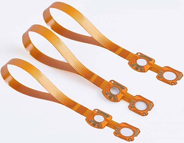
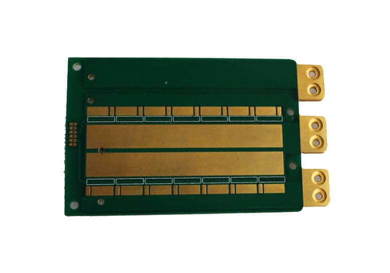
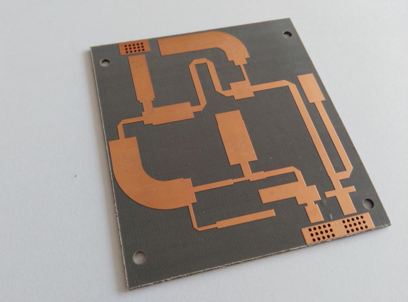
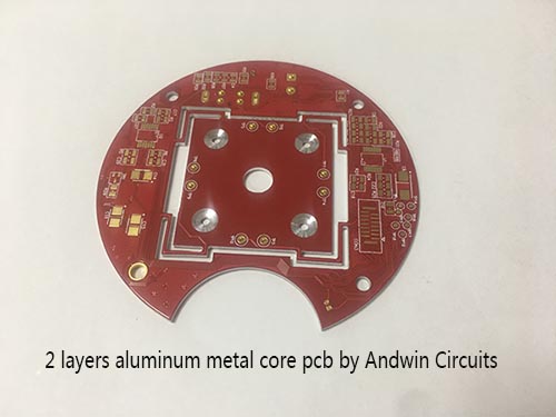
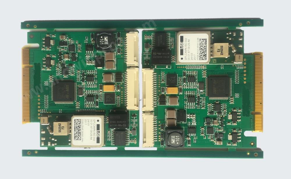
High quality Complex PCB manufacturing
From PCB prototype to volume production
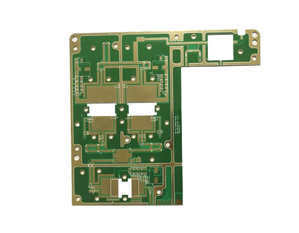
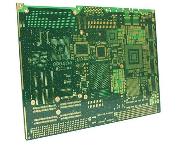
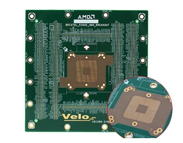
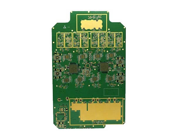
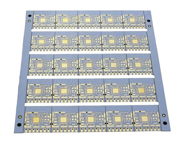
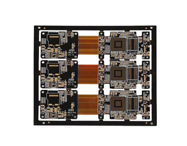
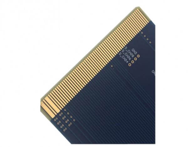
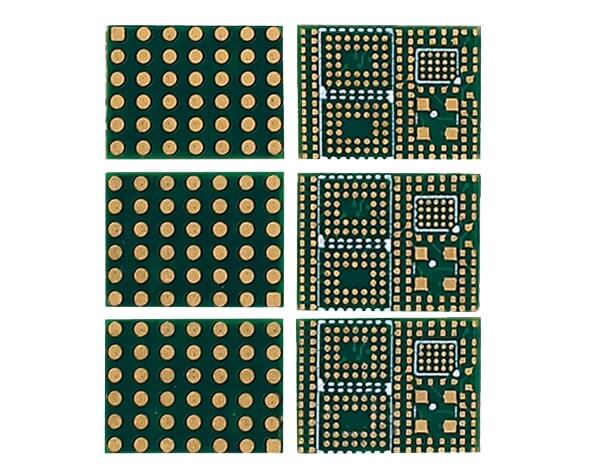
PCB Custom manufacturing
High quality PCB prototype, fast delivery in 12 hours!
1. High quality raw material
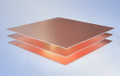
Andwin choose the best raw material for customer to ensure high quality PCB,
KB ShengYi ITEQ ISOLA Rogers TUE Panasonic etc..
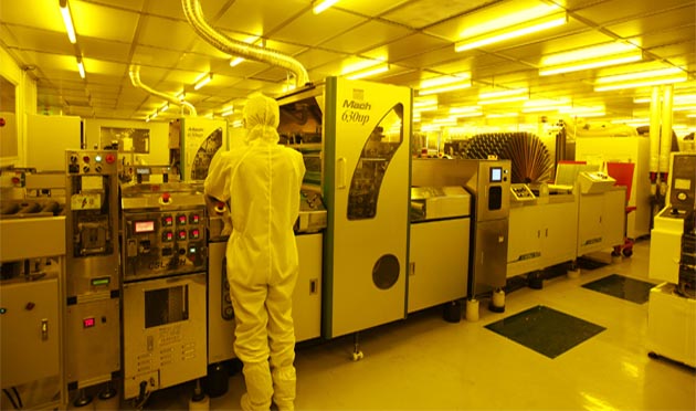
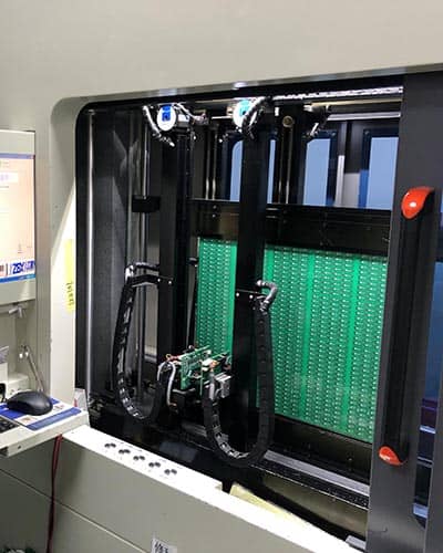
2. Excellent PCB equipment
Better equipments is understructure to do high quality PCB prototype production
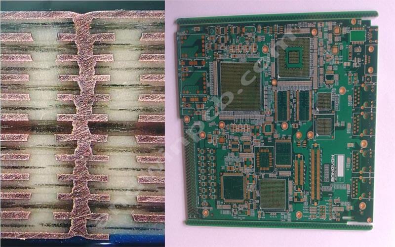
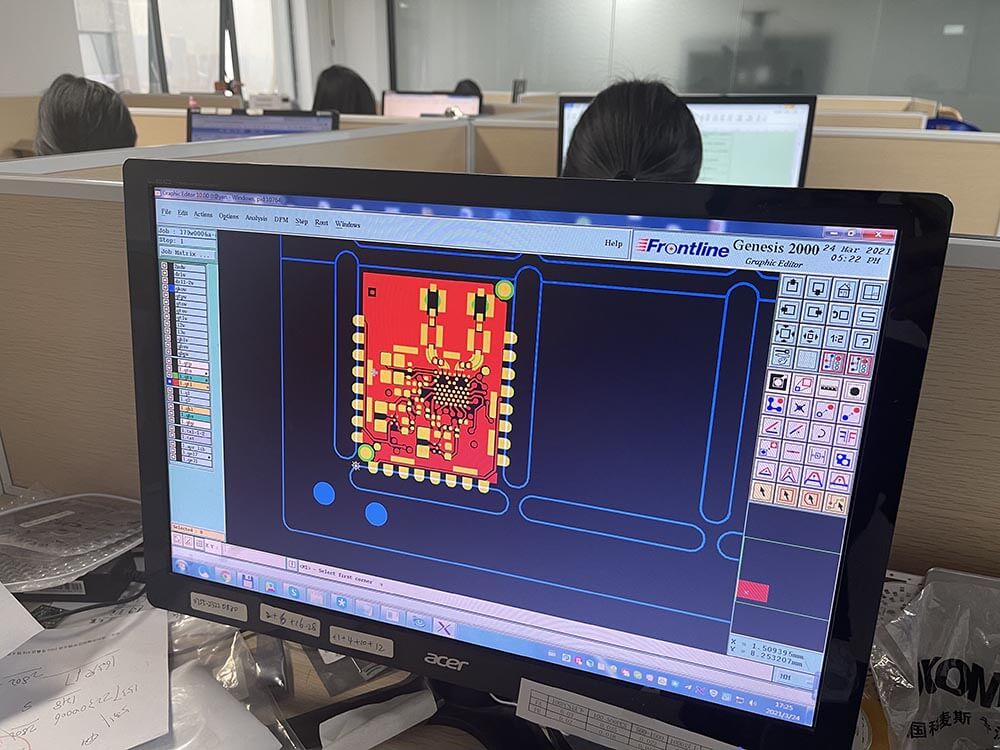
3. DRC and DFM
DRC is the area of Electronic Design Automation that determines
Whether a particular chip layout satisfies a series of recommended parameters called Design Rules.
DRC is a very important step in Printed circuit board (PCB) manufacturing.
Any design from you are always including DRC!
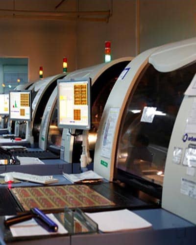
4. A.O.I process
The A.O.I. checks the produced track layout for variances of
The Gerber data, and finds errors the E-Test is not capable to find.
Your multilayers Printed circuit board (PCB) are always including A.O.I.!
5. 100% TEST
Your circuit board (PCB) is checked through a so called
Flying-Probe E-Test Or Fix Tooling E-Test.
The produced PCB is checked by a netlist for short circuits and breaks.
E-Test is very important step in Printed circuit board (PCB) manufacturing.
All boards are always including E-Test!

6. Final Quality Control
Our professional team maintain constant vigilance over our processes,
we know that our products are created with the best possible processes,
And that everything we do conforms to the ISO bodies to which we subscribe.
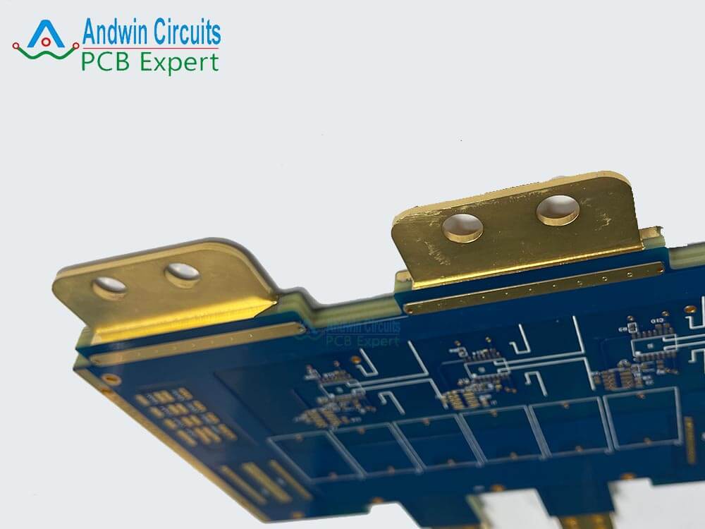
PCB manufacturing Capability

Layers
FR-4 PCB Max. 50 L ( A )

PCB Thickness
Min. 0.35mm Max. 12mm ( A )

Copper Thickness
Out layers ( A ) Min. 8 um Max. 1500um
Inner layers ( B ) Min. 12.5um Max. 1200um

Drill size
Through holes Mechanical drill ( A ) : Min. 0.15mm Max. 6.5mm Tolerance : +/-0.05mm T/D Ratio Max.12:1
Laser drill ( B ): Min. 0.07mm Max. 0.15mm T/D Ratio Max. 1 : 1
Burried Via ( C ): Mechanical drill Min. 0.15mm Max. 0.5mm T/D Ratio Max. 1 : 1
Blind Via ( D ) : Mechanical drill Min. 0.15mm Max. 0.5mm T/D Ratio Max. 1 : 1
Remark: T/D = PCB Thickness/Drill dimension

Line width
Out layer Line Width ( A ) : Min. 0.076mm
Inner layer Line Width ( B ): Min. 0.076mm
Other PCB products, you may interesting