
Design for Test (DFT): Test Points and Boundary Scan in PCB
Design for testability issues cause 35-40% of PCB manufacturing yield losses and extend fault diagnosis from minutes to hours. According to IPC research, boards without proper DFT planning require 3-5× longer testing time and increase field failure rates by 15-25% compared to designs with structured test access. If you want to reduce assembly costs, improve quality control, and accelerate production ramp-up for your electronic products, then you need to implement DFT strategies including test point placement, boundary scan (JTAG), and automated test equipment compatibility from schematic design through PCB layout.
What is Design for Test (DFT) in PCB?
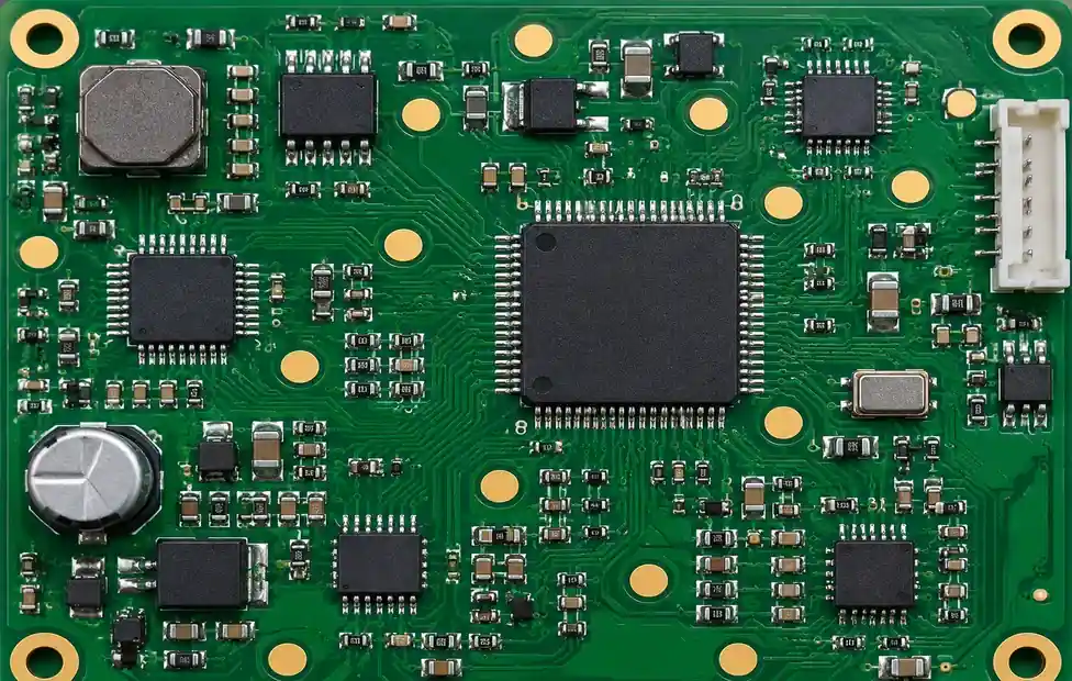
Design for Test (DFT) is a PCB design methodology that ensures boards can be tested efficiently, reliably, and cost-effectively during manufacturing and field diagnostics. DFT incorporates test access features including physical test points, boundary scan architecture (IEEE 1149.1 JTAG), built-in self-test (BIST) circuits, and design rules that enable automated test equipment including in-circuit testers (ICT) and flying probe systems.
The primary goal is to maximize test coverage while minimizing test time and equipment costs. Proper DFT planning during schematic and layout phases prevents expensive board respins, reduces diagnosis time from hours to minutes, and enables production testing at volumes from prototypes to millions of units. Without DFT consideration, even a manufacturable HDI PCB design can become expensive or impossible to test adequately.
You should implement DFT strategies for medium-to-high complexity boards with BGAs, dense component placement, multilayer stackup designs, and applications requiring IPC Class 2 or Class 3 reliability including automotive, medical, aerospace, and telecommunications equipment.
DFT Methods Comparison
| Method | Coverage | Cost | Speed | Best For |
|---|---|---|---|---|
| Test Points + ICT | 85-95% (nets) | Moderate | Fast (15-90s) | Volume >1000/month, fixed design |
| Test Points + Flying Probe | 70-85% (nets) | Lower | Slower (3-10min) | Prototypes, <500 units/month, frequent changes |
| Boundary Scan (JTAG) | 60-80% (device pins) | Low (software) | Medium (30-120s) | Complex digital, BGA-dense, field diagnostics |
| Functional Test | 100% (application) | High | Varies | Validates actual operation, complements structural test |
Test Points: Physical Access for Automated Testing
Test points are exposed copper pads placed on PCB nets to provide physical probe access for in-circuit testing (ICT), flying probe systems, and manual troubleshooting. A properly designed test point allows spring-loaded test probes to make reliable electrical contact without damaging the board or adjacent components.
IPC-2615 specifies test point design requirements: minimum 40 mil (1.0mm) diameter for double-sided probe access, 50 mil (1.27mm) preferred for production reliability. The test point must have no soldermask covering and requires keepout clearance of at least 50 mil (1.27mm) from adjacent pads or components to prevent probe damage or false contacts during testing.
Test Point Placement Strategy
Not every net requires a test point. Critical nets for test access include: all power rails (Vcc, Vdd, GND), IC enable and reset signals, clock distribution networks, communication buses (SPI, I2C, UART, USB), high-speed differential pairs, analog sensor outputs, and any net without existing boundary scan coverage. Connector pins, component leads, and vias can serve as test points if they meet size and clearance requirements.
Strategic placement reduces test point count by 30-50% while maintaining coverage. Place test points on the bottom side when top side has high component density. Distribute test points to balance fixture probe pressure across the board, preventing board warpage during ICT testing. For boards requiring both ICT and flying probe testing, ensure test points remain accessible from both sides.

ICT vs Flying Probe Test Access Requirements
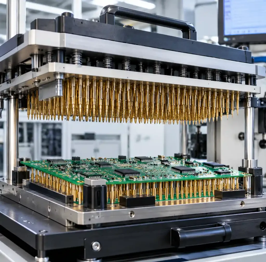
In-circuit testing uses a bed-of-nails fixture with fixed probe positions, testing 200-400 nets simultaneously in 15-90 seconds per board. ICT requires precise test point positioning on a 50 mil (1.27mm) or 100 mil (2.54mm) grid for probe alignment. Fixture cost ranges from $3,000-15,000 but amortizes across production volumes exceeding 1,000 units monthly. ICT delivers 90-95% net coverage and detects component value errors, shorts, opens, and incorrect part placement.
Flying probe testing uses two to six motorized probes that move sequentially to each test point, eliminating fixture costs. This enables cost-effective testing for prototypes and production volumes under 500 units monthly where fixture investment cannot be justified. Flying probe requires only 40-60 mil (1.0-1.5mm) test point diameter with 80 mil (2.0mm) clearance, offering greater layout flexibility than ICT. Test time ranges from 3-10 minutes per board depending on net count and probe quantity.
Choose ICT when: production volume exceeds 1,000 units monthly, design is stable with minimal ECOs, test time under 90 seconds is required, and fixture cost amortizes favorably. Choose flying probe when: prototype or NPI builds under 500 units, design changes occur frequently, board has insufficient test access for ICT fixture probing, or multiple product variants share common testing requirements.
Boundary Scan (JTAG): IEEE 1149.1 Testing
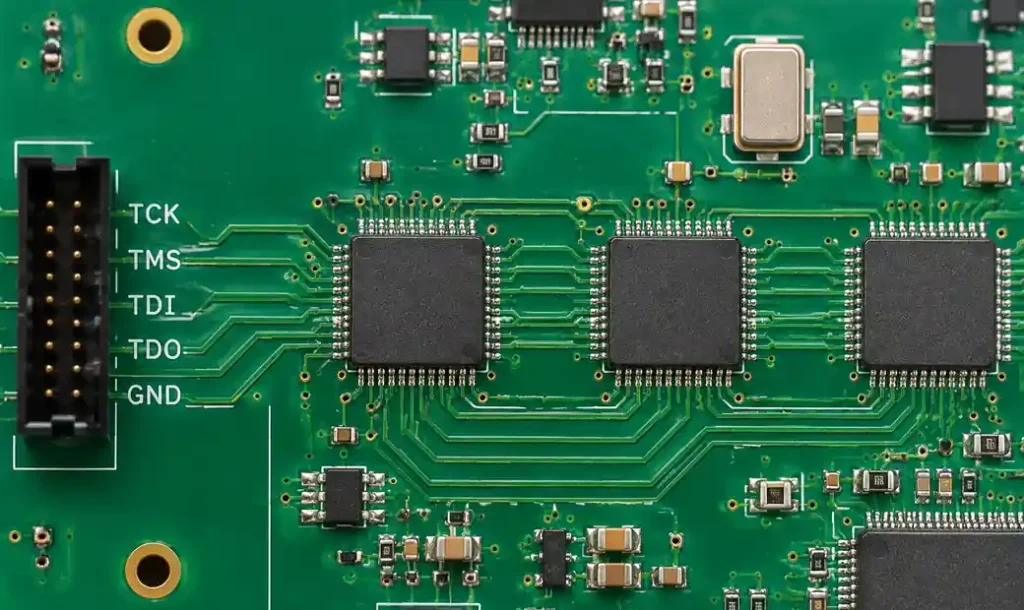
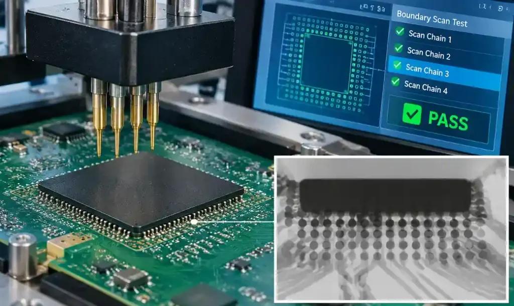
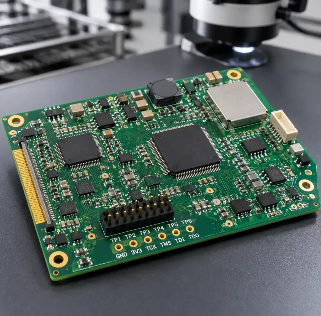
Boundary scan is a structural test method defined by IEEE 1149.1 standard that enables internal testing of digital ICs and interconnect verification without physical test probes. JTAG-compliant devices contain boundary scan registers on every I/O pin, allowing test patterns to be shifted serially through a dedicated Test Access Port (TAP) consisting of four required signals: TDI (Test Data In), TDO (Test Data Out), TCK (Test Clock), and TMS (Test Mode Select), plus optional TRST (Test Reset).
The boundary scan chain allows one JTAG device to drive signals onto PCB nets while another JTAG device observes those signals, testing interconnects independently of the application firmware. This capability proves essential for BGA packages where solder joints remain hidden under the component body, making physical probing impossible. Boundary scan achieves 60-80% test coverage on boards with sufficient JTAG device density, complementing rather than replacing physical test points.
JTAG Chain Design Requirements
Connect JTAG devices in a daisy-chain topology: TDO of device 1 connects to TDI of device 2, continuing through all JTAG devices, with the final TDO connecting to the test controller. All devices share common TCK, TMS, and optional TRST signals. IPC-7351 recommends 50-100 ohm controlled impedance for TCK to maintain signal integrity across multiple devices, particularly when clock frequency exceeds 10 MHz.
Design considerations: place JTAG connector near the scan chain entry point to minimize routing. Add 1kΩ pull-up resistors on TMS, TDI, and TDO to prevent floating during power-up. Include 10kΩ pull-up on TRST if used. Keep TCK trace length under 12 inches total for reliable operation above 10 MHz. Avoid sharing JTAG signals with functional application connections to prevent test interference. Series termination resistors (22-33Ω) on TCK near the driving source reduce reflections in long chains.
Boundary Scan Test Coverage
Boundary scan effectively tests: interconnects between JTAG devices (shorts, opens, incorrect connections), JTAG device I/O functionality, memory devices connected to JTAG controllers (through BSDL-defined memory access), and some non-JTAG devices when driven and observed by JTAG-enabled devices. Coverage depends on JTAG device density: boards with ≥60% digital ICs supporting boundary scan achieve 70-80% structural test coverage.

Boundary scan cannot test: analog circuits, power supply sequencing, precise analog voltage levels, RF signal paths, or interconnects between non-JTAG devices with no JTAG device observation. Complement boundary scan with analog test points on critical analog nets including voltage regulators, ADC inputs, DAC outputs, temperature sensors, and current monitoring circuits.
Test Point Design Rules and Specifications
| Parameter | ICT (Bed-of-Nails) | Flying Probe | Manual Probe | Standard |
|---|---|---|---|---|
| Min Diameter | 50 mil (1.27mm) | 40 mil (1.0mm) | 35 mil (0.9mm) | IPC-2615 |
| Clearance | 100 mil (2.54mm) | 80 mil (2.0mm) | 60 mil (1.5mm) | IPC-2615 |
| Grid Alignment | 50 mil or 100 mil | Off-grid OK | Off-grid OK | Fixture-dependent |
| Soldermask | No coverage | No coverage | No coverage | IPC-SM-840 |
| Finish | ENIG, OSP, HASL | ENIG, OSP, HASL | ENIG, OSP, HASL | IPC-4552 |
Probe Pad Surface Finish Selection
Test point surface finish must withstand repeated probe contact (10,000-100,000 cycles) without degradation. ENIG (Electroless Nickel Immersion Gold) provides the best probe durability with flat, solderable surface and excellent contact resistance (2-5 mΩ). OSP (Organic Solderability Preservative) offers lower cost but limited probe cycle life (1,000-5,000 cycles), suitable for prototypes and low-volume production. HASL (Hot Air Solder Leveling) creates non-planar surface with variable height (±75μm), causing probe alignment issues in dense ICT fixtures.
For production volumes exceeding 5,000 units, specify ENIG on test points even if the board uses OSP globally. Selective ENIG on test pads adds $0.50-2.00 per board but prevents probe wear failures and maintains consistent contact resistance throughout production runs. Quick turn PCB prototypes can use OSP universally to minimize cost and lead time.
DFT Implementation Strategy
Implement DFT in three phases: schematic review, PCB layout, and manufacturing verification. During schematic design, select JTAG-capable devices when equivalent non-JTAG parts exist at similar cost. Add JTAG header connector to design. Identify critical nets requiring test access: power supplies, reset signals, clock distribution, communication interfaces, and signals with no boundary scan visibility.
Schematic-Level DFT Planning
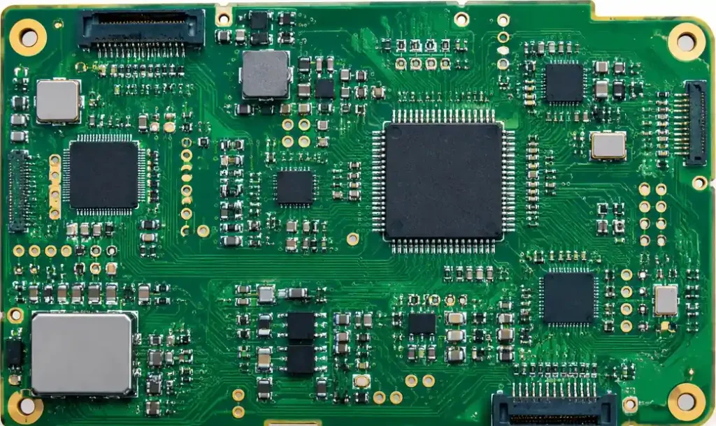
Add test points to schematic as dedicated components (test pad symbols) rather than adding them ad-hoc during layout. This ensures test access requirements receive proper design review and appear on assembly drawings. For each power rail, specify at least one test point per voltage domain. For differential pairs and high-speed signals, place test points on both P and N nets to enable TDR (Time Domain Reflectometry) and eye diagram measurements.
Include pull-up or pull-down resistors on test points for floating nets after component removal or during boundary scan testing. Document test point requirements in design notes: “TP1-TP50: 50 mil dia, ENIG finish, bottom side, 100 mil clearance per IPC-2615.” This specification ensures CM and test vendors understand requirements without ambiguity.
Layout-Level DFT Guidelines
Reserve test point keepout zones during component placement before routing begins. Distribute test points across board area to balance ICT fixture probe pressure and prevent board flexing during testing. Group test points by circuit function (power, digital I/O, analog, communication) to simplify test program development and fixture wiring.
Avoid placing test points under components, even with bottom-side access, as this complicates rework and field diagnostics. Maintain 100 mil (2.54mm) minimum spacing between adjacent test points for ICT fixtures. When board density prevents proper spacing, consider double-sided test point strategy or flying probe testing instead of ICT.
For HDI designs with microvias and fine-pitch BGAs, specify flying probe testing early in the design phase to relax test point spacing requirements from 100 mil to 80 mil, gaining valuable routing channels. Document test point locations in fabrication drawing layers using industry-standard test point symbols from IPC-2581 or ODB++ formats.
Combining DFT Methods for Maximum Coverage
No single test method achieves 100% fault coverage economically. Optimal DFT strategy combines multiple approaches: physical test points for analog circuits and power supplies, boundary scan for dense digital interconnects under BGAs, and functional testing for application-level validation. This hybrid approach delivers 95-98% total fault coverage while minimizing cost per test.
Example strategy for complex automotive PCB: flying probe tests 120 analog and power nets (40% of nets) in 8 minutes, boundary scan tests 280 digital interconnects between three JTAG devices (55% of nets) in 90 seconds, functional test validates CAN bus communication and sensor outputs in 3 minutes. Total test time: 12 minutes per board with 96% fault coverage at IPC Class 3 requirements.
DFT Cost-Benefit Analysis
Test access costs $0.10-0.50 per test point for layout area and routing complexity. ICT fixture costs $3,000-15,000 amortized over production volume. Flying probe testing costs $30-80 per hour machine time. Boundary scan requires BSDL files (free from IC vendors) and test software ($2,000-10,000 one-time). Compare these costs against field failure costs: warranty returns ($50-200 per unit), reputation damage, and product recalls.
Industry data shows proper DFT implementation reduces field failures by 15-25% and manufacturing test time by 40-60%. For production volumes exceeding 5,000 units, DFT investment delivers ROI within the first 2,000-3,000 units through reduced test time, improved yield, and lower field failure rates. Even for prototypes, DFT accelerates board bring-up and reduces debug time from days to hours.
DFT for Different PCB Applications
Medical device PCBs require IPC-6012 Class 3 reliability and traceability. Implement comprehensive test point coverage (90%+ nets), boundary scan on all JTAG-capable devices, and functional testing that validates safety-critical parameters. Document test coverage in design history file (DHF) for FDA 21 CFR Part 820 compliance. Test points must use ENIG finish for long-term reliability and resistance to corrosion from cleaning processes.
Automotive electronics following IATF 16949 standards require production testing with statistical process control. Use ICT fixtures for volumes exceeding 10,000 units monthly, achieving 90-second test times for real-time production line integration. Boundary scan enables field diagnostics through OBD-II connector access, reducing warranty diagnosis costs. Include test points for power supply monitoring (battery voltage, 5V/3.3V rails), CAN bus termination verification, and sensor signal validation.
Consumer electronics and IoT devices with frequent design iterations benefit from flying probe testing flexibility. Specify 40 mil test points with 80 mil clearance to maximize routing density while maintaining test access. Use boundary scan on processor, FPGA, and memory devices to verify BGA solder quality without physical access. Implement BIST (Built-In Self-Test) routines in firmware to complement structural testing with application-level validation.
Frequently Asked Questions About DFT and Test Points
What percentage of nets need test points?
Target 70-90% net coverage for production boards depending on volume and reliability requirements. Power rails, resets, clocks, and communication buses require test points. Skip test points on nets fully covered by boundary scan or nets with existing probe-accessible component leads. IPC-6012 Class 3 applications target 85-90% coverage.
Can vias serve as test points?
Vias can serve as test points if they meet minimum diameter (40 mil) and clearance (60-80 mil) requirements and have no soldermask covering. Via-in-pad designs with resin plugging cannot serve as test points due to non-conductive fill. Through-hole vias with 0.020″ (0.5mm) diameter work for flying probe but not for ICT fixtures which require 50 mil minimum.
How many JTAG devices are needed for effective boundary scan testing?
Boundary scan becomes cost-effective when ≥3 JTAG devices exist on the board, enabling mutual interconnect testing between devices. Maximum effectiveness occurs when 60-80% of ICs support JTAG. Single JTAG device provides limited value beyond programming and debug access.
What is the cost difference between ICT and flying probe testing?
ICT fixture costs $3,000-15,000 (one-time) but tests boards in 15-90 seconds at $1-3 per test. Flying probe has no fixture cost but tests boards in 3-10 minutes at $0.50-1.50 per minute ($1.50-15 per test). ICT becomes cost-effective above 1,000-2,000 units per design. Flying probe suits prototypes and volumes under 500 units monthly.
Do test points affect signal integrity on high-speed nets?
Test point capacitance (0.2-0.5 pF) and stub length affect impedance on controlled impedance traces. For signals <1 GHz, impact is negligible. For 10+ Gbps signals, keep test point stub length under 10 mil or place test points in series with the trace (inline) rather than as a stub. Use controlled impedance design rules to minimize discontinuity. Some designers omit test points on critical high-speed nets, accepting reduced test coverage for signal integrity preservation.
Can boundary scan replace all physical test points?
No. Boundary scan tests only digital interconnects between JTAG devices. Physical test points remain essential for: analog circuits, power supply voltages, non-JTAG devices, and nets without JTAG device connection. Optimal DFT combines boundary scan (60-80% digital coverage) with strategic test points (analog, power, critical signals) for 95%+ total coverage.
Conclusion
Design for Test implementation reduces manufacturing costs, improves first-pass yield, and enables field diagnostics throughout product lifecycle. Strategic test point placement following IPC-2615 guidelines, JTAG boundary scan architecture for dense BGA assemblies, and proper test method selection (ICT vs flying probe) based on production volume deliver 95%+ fault coverage while minimizing test time and equipment investment.
If you need PCB manufacturing with expert DFT support for your electronic devices, Andwin Circuits offers comprehensive design review, test point optimization, and JTAG integration services. Our facility manufactures boards up to 50 layers with fast 7-day turnaround for prototypes and production volumes. We provide DFT consultation during schematic review, layout verification, and first-article testing with detailed coverage reports meeting IPC Class 2 and Class 3 requirements for automotive, medical, industrial, and consumer electronics.
Contact us today for PCB manufacturing with integrated DFT services, test strategy recommendations, and competitive factory-direct pricing for your next project.