
Controlled Impedance PCB Design: Calculation and Testing Methods
If you route USB 3.x, DDR, PCIe, or RF signals, then a trace is no longer a wire. It is a transmission line, and its impedance decides whether your eye diagram stays open or your link throws bit errors. Even a 10-15% mismatch between trace impedance and the driver can create reflections strong enough to close an eye diagram.
Here is the part most guides skip: your layout only sets the target. The fab shop sets the result. This article shows how impedance is calculated, why the real board drifts from the calculator, and how controlled impedance PCB fabrication is verified with TDR.
What Is Controlled Impedance?
Controlled impedance means the characteristic impedance (Z0) of a trace is held to a defined target and tolerance along its entire length. Common targets are 50Ω single-ended, 90Ω for USB differential pairs, and 100Ω for DDR and LVDS differential lines.
Z0 is set by trace geometry, the distance to the reference plane, and the dielectric constant (Dk) of the material. It has nothing to do with trace length. A 3mm trace and a 300mm trace hit the same Z0 if their cross-section matches.
You need it once edge rates get fast, roughly above 1 GHz or with rise times under 1ns. Below that, parasitics are negligible and a normal trace is fine.
Single-Ended vs Differential Impedance
Single-ended impedance measures one trace against a reference plane. Differential impedance measures the coupled behavior of a pair carrying equal, opposite signals. The two are not interchangeable, and coupling makes differential impedance lower than twice the single-ended value.
| Parameter | Single-Ended | Differential |
|---|---|---|
| Reference | One trace to plane | Two coupled traces |
| Typical target | 50Ω (±10%) | 90Ω / 100Ω (±10%) |
| Key variable | Width, height, Dk | Above + pair spacing |
| Common signals | Clocks, single lines | USB, DDR, PCIe, LVDS |
| Noise immunity | Lower | Higher (common-mode reject) |
Specify differential pairs by both the differential target and the spacing that produces it. Never let routing tools default the gap.
Impedance Calculation Methods
The classic IPC-2141 microstrip approximation is a useful starting point:
Z0 = 87 / √(εr + 1.41) × ln(5.98H / (0.8W + T))
Here H is dielectric height, W is trace width, T is copper thickness, and εr is the dielectric constant. The formula shows the levers clearly: thinner dielectric or wider traces lower Z0; higher Dk lowers it too.
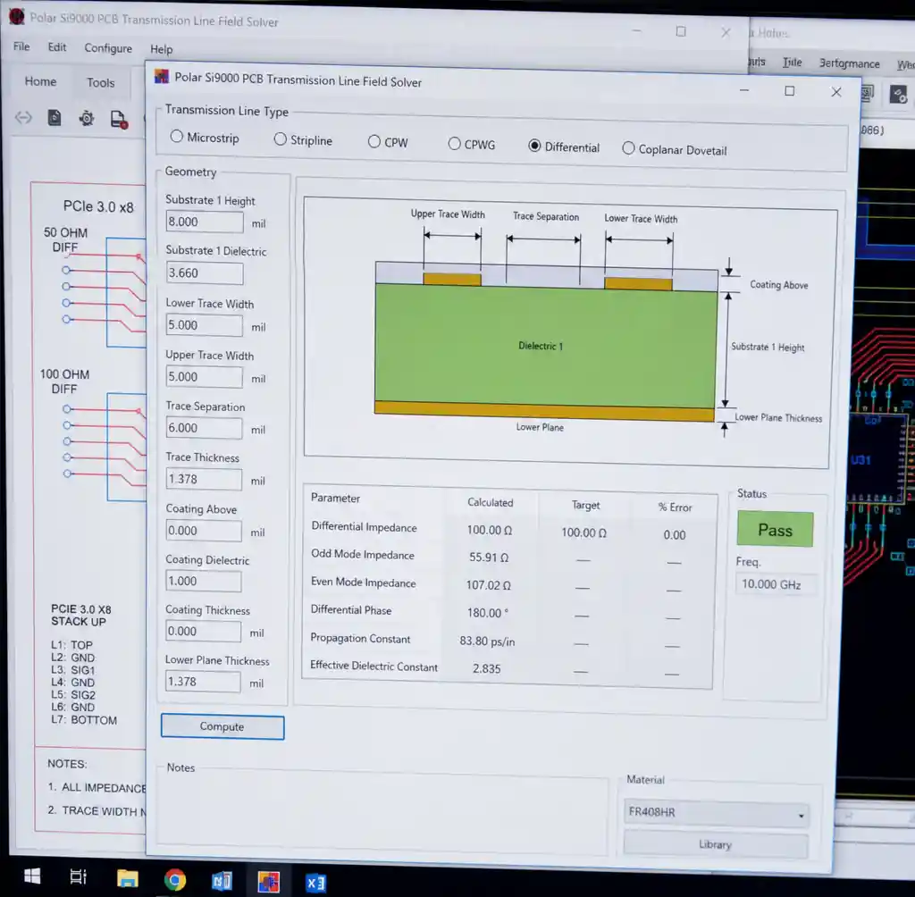
These closed-form equations are accurate to roughly ±5-10%, which is not tight enough for production. Field-solver tools like Polar Si9000 or Saturn PCB Toolkit model the real trapezoidal cross-section and are what fabs actually use. Treat hand formulas as a sanity check, not a spec.
What Actually Sets Your Impedance
Four inputs dominate the finished result: conductor cross-section, distance to the reference plane, dielectric properties, and pair spacing for coupled lines. The table below shows how each variable pushes Z0.
| Variable | Change | Effect on Z0 |
|---|---|---|
| Trace width | Wider | Decreases |
| Dielectric height | Thicker | Increases |
| Dielectric constant (Dk) | Higher | Decreases |
| Copper thickness | Thicker | Slightly decreases |
| Pair spacing (diff) | Wider | Increases |
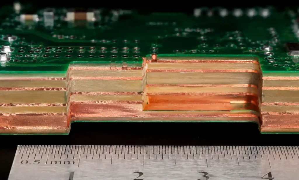
Because these interact, always fix the impedance in the PCB stackup first, then let trace width follow. Designers who pick a “standard” width and hope for the best get boards that miss target on half their layers.
The Factors Most Designers Miss
This is where calculator values and real boards part ways. From the fabrication floor, these are the culprits behind failed TDR reports.
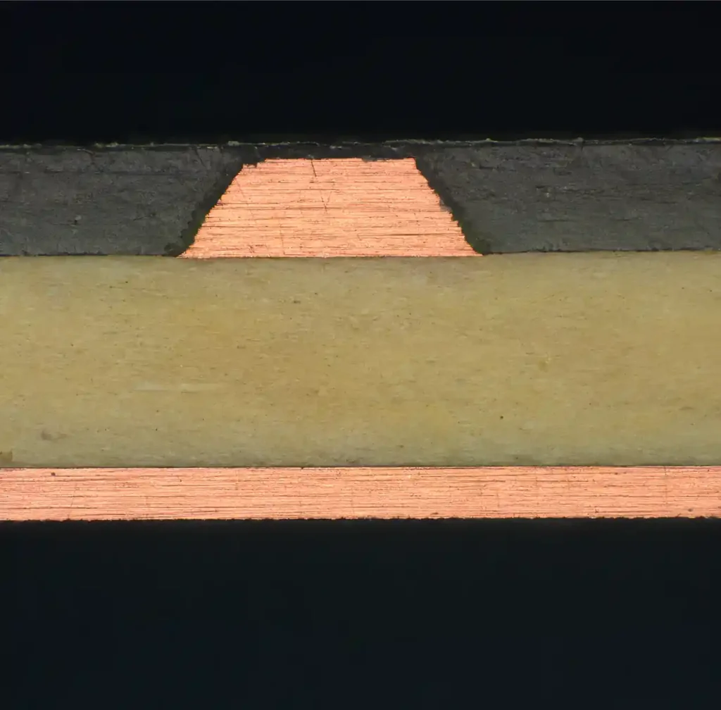
Etched copper is trapezoidal, not rectangular. Etching undercuts the trace, so the bottom is wider than the top. This etch factor shifts effective width and raises Z0 if your design assumed a clean rectangle. Give the fab your target Z0 and let them adjust width to their process.
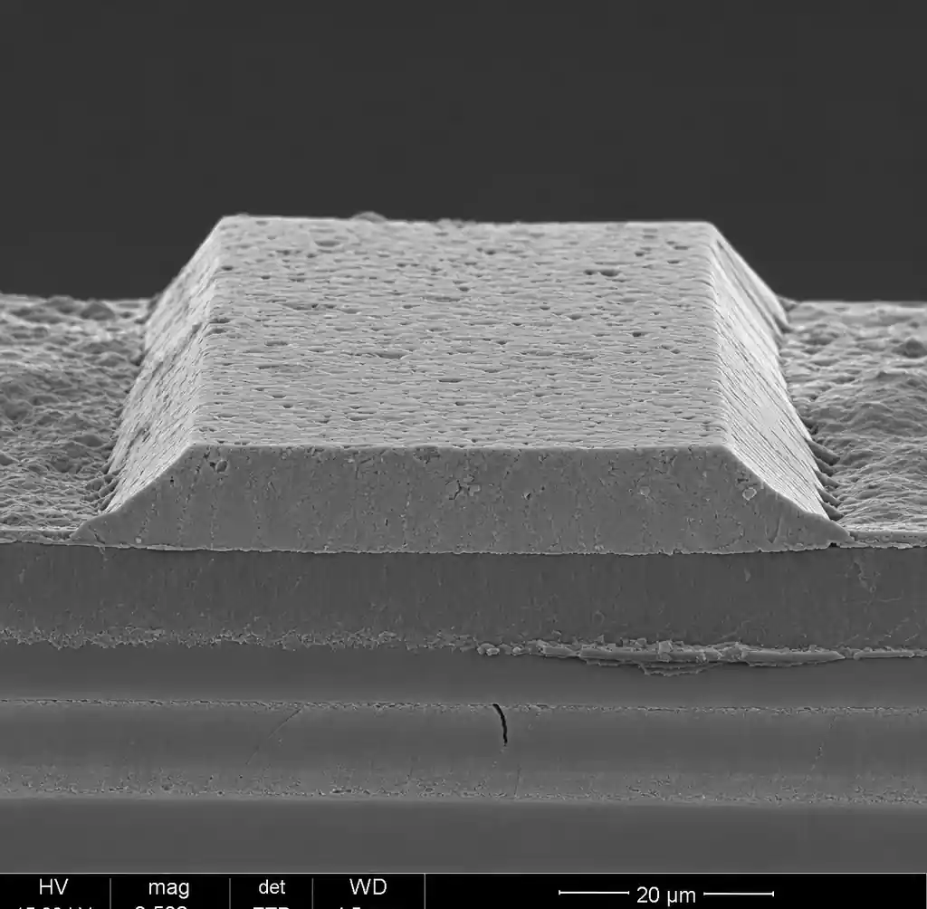
Copper roughness lowers effective impedance and adds loss. Reference planes are deliberately roughened for lamination bonding. At GHz frequencies the signal travels along that rough surface, increasing effective path length and insertion loss.
Solder mask changes surface microstrip. A mask layer over an exposed trace adds dielectric and drops Z0 by 2-3Ω. Tell your fab whether coupons are masked so the measurement matches the design.
Resin content varies by copper distribution. Prepreg squeezes differently under dense versus sparse copper during pressing, so dielectric height, and therefore Z0, can drift across one panel.
Manufacturing Tolerances and Cost
Tolerance is a commercial decision, not just a technical one. Tighter control means more test coupons, tighter etch windows, and higher scrap. The typical market pricing looks like this:
| Tolerance | Cost Premium | Typical Use |
|---|---|---|
| ±10% | Baseline | Most digital, DDR, USB |
| ±7% | +10-15% | Faster interfaces |
| ±5% | +20-40% | RF, high-speed SerDes, IC test boards |
Do not over-specify. A 3-inch USB 3.0 trace usually meets spec at ±8%, so demanding ±5% wastes money without improving the link. Calculate the tolerance your rise time actually needs.
TDR Testing Methods
Time-Domain Reflectometry (TDR) is the standard verification method per IPC-TM-650 2.5.5.7. A TDR launches a fast step edge down the trace and measures reflections; any impedance change appears as a bump on the waveform. Impedance is read at the trace midpoint, away from launch discontinuities.
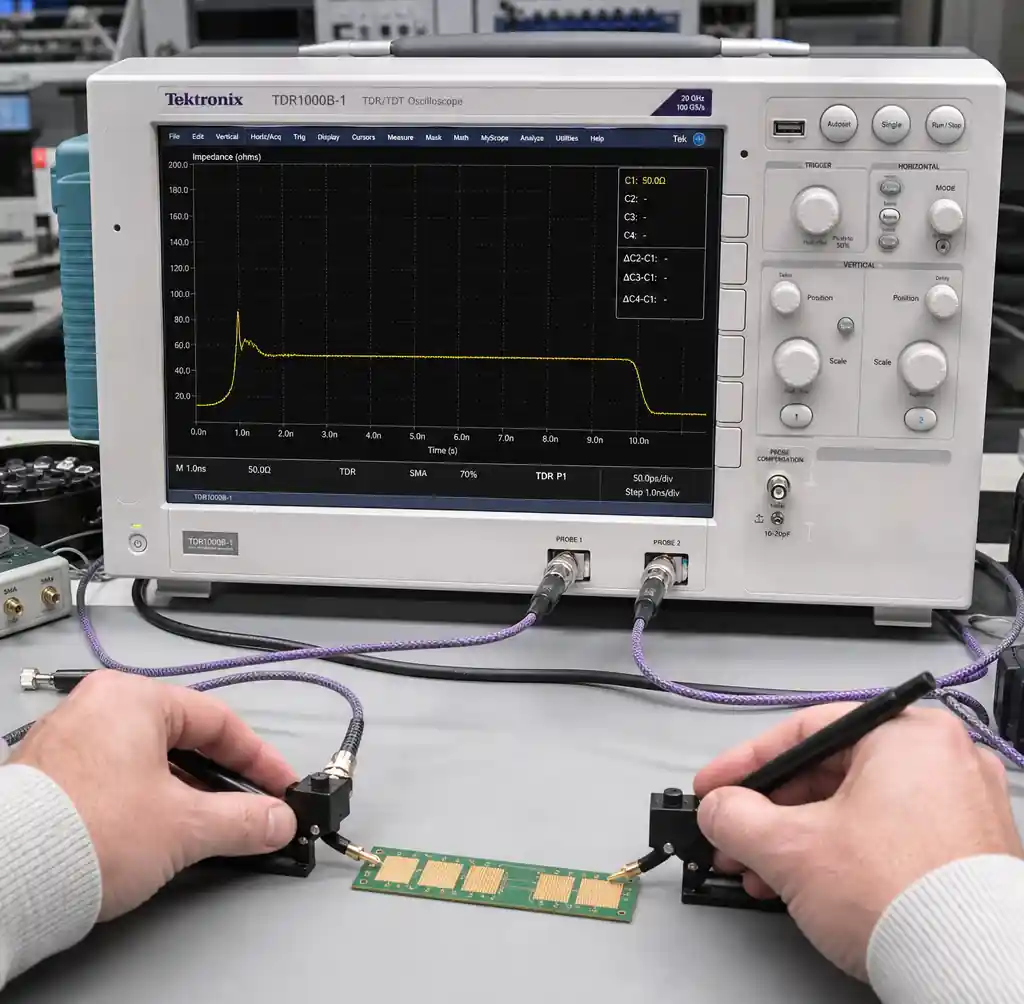
Fabs do not probe your live nets. They add an impedance test coupon to the panel border, built with the same stackup and trace widths as your controlled nets. The coupon is measured after fabrication and represents the real board. A key detail: the TDR rise time must be fast enough to resolve short traces, and single-ended versus differential coupons are measured differently.
Ask for the TDR report and coupon data with your boards. Reputable PCB E-test services deliver it as standard proof, not on request.
Design Best Practices
Follow these steps to hit target the first time, whether on rigid or rigid-flex boards:
- Define impedance targets per net class before layout.
- Design the stackup with your fab, then derive trace widths from it.
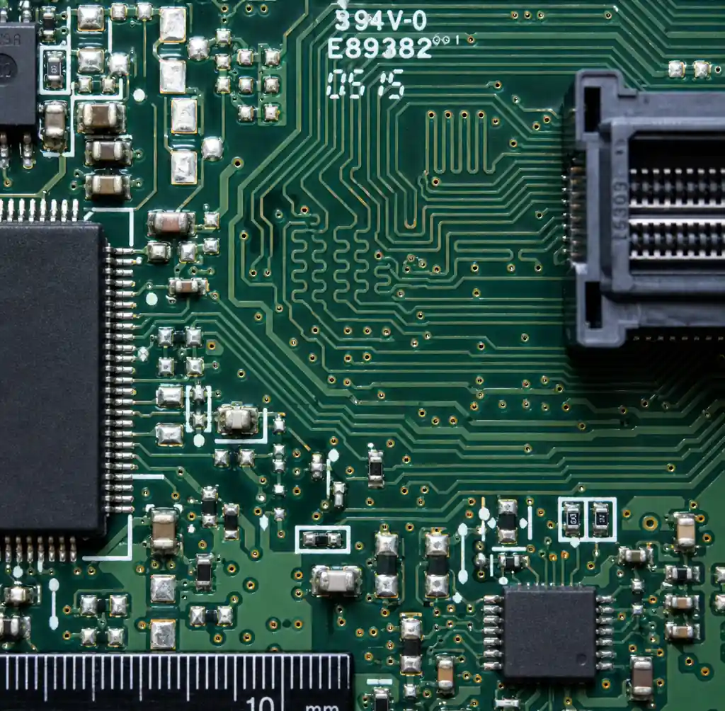
- Keep a continuous reference plane directly under every controlled trace.
- Never route a high-speed signal across a plane split or gap.
- Match differential pair length and maintain constant spacing.
- Send the fab your Z0 target and tolerance, not just a fixed width.
- Require a TDR coupon report for release.
These practices apply across HDI, telecom, and high-speed digital designs. For deeper layer planning, see our PCB layer stackup guide.
FAQs
What is a good impedance tolerance for most designs?
±10% is the industry baseline per IPC-6012 and works for most DDR, USB, and digital interfaces. Move to ±5% only for RF or high-speed SerDes links.
Does trace length affect impedance?
No. Characteristic impedance depends on cross-section geometry and material, not length. Length affects delay and loss, not Z0.
Why does my board measure different from my calculator?
Etch factor, copper roughness, solder mask, and resin flow shift the real value. Field solvers and fab process data are more accurate than hand formulas.
Can I get impedance control on a 4-layer board?
Yes. A standard 4-layer stackup with defined dielectric heights supports 50Ω and 100Ω routing at baseline cost.
How is differential impedance measured?
With a differential TDR on a matched coupon, driving equal and opposite edges into the pair and reading impedance at the midpoint.
Conclusion
Controlled impedance is a partnership between your layout and your fabricator. You define the targets and reference planes; the shop controls etch, pressing, and roughness to land the number. The traps that sink real boards, trapezoidal traces, copper roughness, solder mask, and plane splits, live between those two roles, so specify Z0 and tolerance clearly and demand TDR coupon proof.
Andwin Circuits manufactures controlled impedance PCBs up to 50 layers with ±10% standard and ±5% tight tolerance, verified by TDR testing on every panel, with fast delivery in 7 days. Contact us today for impedance-controlled PCB manufacturing and factory-direct pricing.