
High-Frequency PCB Design: Material Selection and Layout Techniques
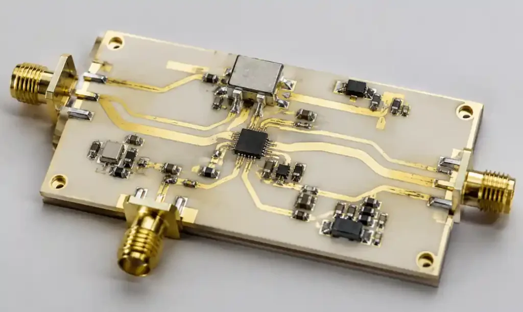
High-frequency circuits operating above 1 GHz power 5G infrastructure, radar systems, and satellite communications. At these frequencies, every trace becomes a transmission line where a single impedance mismatch can degrade signal performance by 3dB or more. Industry data shows that 40% of RF design failures trace back to improper material selection or layout errors.
If you want to design RF and microwave PCBs that meet specifications from the first build, you must understand dielectric properties, controlled impedance design, via management, and electromagnetic coupling. This guide provides practical design rules for circuits from 1 GHz to 77 GHz based on current manufacturing capabilities and test data.
What Is High-Frequency PCB Design?
High-frequency PCB design addresses circuits where signal wavelengths approach trace dimensions, typically starting above 500 MHz. At 10 GHz, the electrical wavelength in standard FR-4 is approximately 10mm, making a 5mm trace exactly one-half wavelength long—a resonant structure that radiates energy and disrupts signal integrity.
These designs require controlled impedance transmission lines, low-loss dielectric materials, and careful via design. Unlike digital circuits where logic levels tolerate significant noise margins, RF signals operate with power budgets measured in dBm where every 0.1dB insertion loss matters. You should apply high-frequency design principles when working above 1 GHz, with marginal designs from 500 MHz to 1 GHz, and relaxed requirements below 500 MHz.
Why Material Selection Determines RF Performance
Standard FR-4 exhibits dielectric constant (Dk) variations of ±10% across frequency and temperature. This instability translates directly to impedance variations—feeding incorrect Dk values into your impedance calculator produces 50Ω traces that measure 46Ω or 54Ω after fabrication, failing specification before via and connector losses are added.
The dissipation factor (Df) quantifies how much signal energy converts to heat as it propagates through the dielectric. FR-4 exhibits Df of 0.015-0.020 at 10 GHz, while Rogers RO4350B maintains 0.0037 at the same frequency—an 80% reduction in dielectric loss. Over a 100mm trace at 10 GHz, this difference represents 0.5dB additional insertion loss with FR-4.
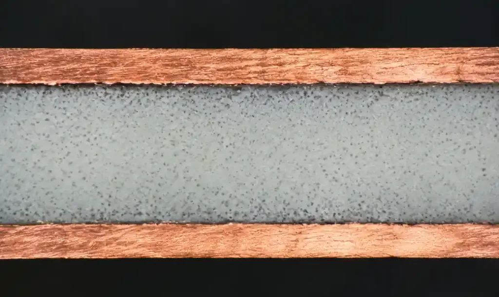
Copper surface roughness creates an often-overlooked loss mechanism. At microwave frequencies, current flows in a thin skin depth—just 0.66 micrometers at 10 GHz. Standard electrodeposited copper with 8-10 micrometer peak-to-valley roughness dramatically increases effective resistance through the “snowplow effect” where current must travel a longer path around surface irregularities. Specifying reverse-treated foil or very-low-profile (VLP) copper reduces conductor loss by 20-30% above 5 GHz.
Rogers Materials: Industry Standards for RF Design
Rogers Corporation high-frequency laminates dominate RF PCB manufacturing because they deliver predictable electrical properties. The three most common series cover different application needs and cost points.
Rogers RO4000 series uses hydrocarbon ceramic formulations providing Dk from 3.3 to 3.7 with ±2% tolerance. RO4003C (Dk=3.38, Df=0.0027 at 10 GHz) offers the best balance of electrical performance and processability, using standard FR-4 fabrication equipment. RO4350B (Dk=3.48, Df=0.0037 at 10 GHz) provides better thermal stability for applications with high power dissipation.
Rogers RO3000 series delivers lower loss for demanding microwave applications. RO3003 (Dk=3.00, Df=0.0010 at 10 GHz) suits antenna feeds and low-noise amplifier circuits where every 0.1dB matters. These PTFE-based materials require specialized drilling and routing due to their soft, deformable nature.
| Material Series | Dk @ 10 GHz | Df @ 10 GHz | Tg (°C) | Applications |
|---|---|---|---|---|
| Rogers RO4003C | 3.38 ±0.05 | 0.0027 | >280 | General RF, microwave |
| Rogers RO4350B | 3.48 ±0.05 | 0.0037 | >280 | High-power RF |
| Rogers RO3003 | 3.00 ±0.04 | 0.0010 | >500 | Low-loss microwave |
| Taconic RF-35 | 3.50 ±0.05 | 0.0018 | >300 | Military, aerospace |
Taconic and Isola also manufacture RF laminates with comparable performance. Material selection should balance electrical requirements, thermal demands, mechanical constraints, and cost. For prototypes below 6 GHz, you can use high-quality FR-4 with Dk=4.2-4.4 and Df<0.01, accepting slightly higher loss and tighter tolerance control during fabrication.
Controlled Impedance Design and Stackup
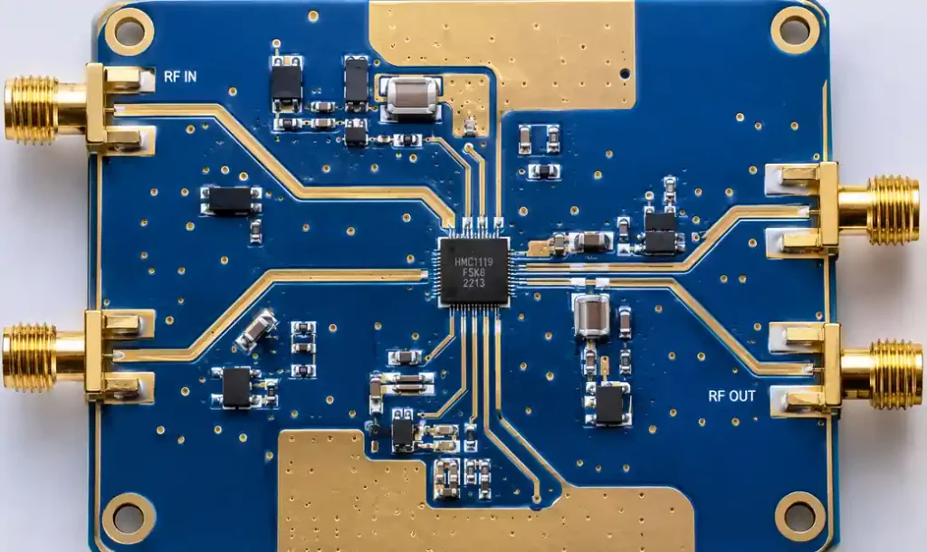
Microstrip and stripline represent the two fundamental transmission line structures in RF PCBs. Microstrip places the signal trace on an outer layer with a ground plane beneath it, offering easy access for tuning and probing. Stripline sandwiches the signal trace between two ground planes, providing superior noise immunity and no radiation—critical for dense layouts with multiple RF channels.
Calculate trace width using proven field solvers, not approximations. For 50Ω microstrip on 0.5mm thick RO4003C with 1oz copper, the trace width is approximately 1.1mm. The same impedance in stripline requires narrower traces because of the dual-plane capacitance. Always verify calculations with your PCB manufacturer’s impedance test coupons.
Specify controlled impedance tolerance per IPC-2141. Class 2 requires ±10% impedance tolerance (45-55Ω for 50Ω nominal), suitable for most RF designs below 10 GHz. Class 3 tightens to ±5%, necessary for millimeter-wave applications where small deviations cause measurable insertion loss. Manufacturers achieve tighter tolerances through test coupons measuring actual fabricated impedance, adjusting trace widths on production panels to compensate for dielectric thickness variations.
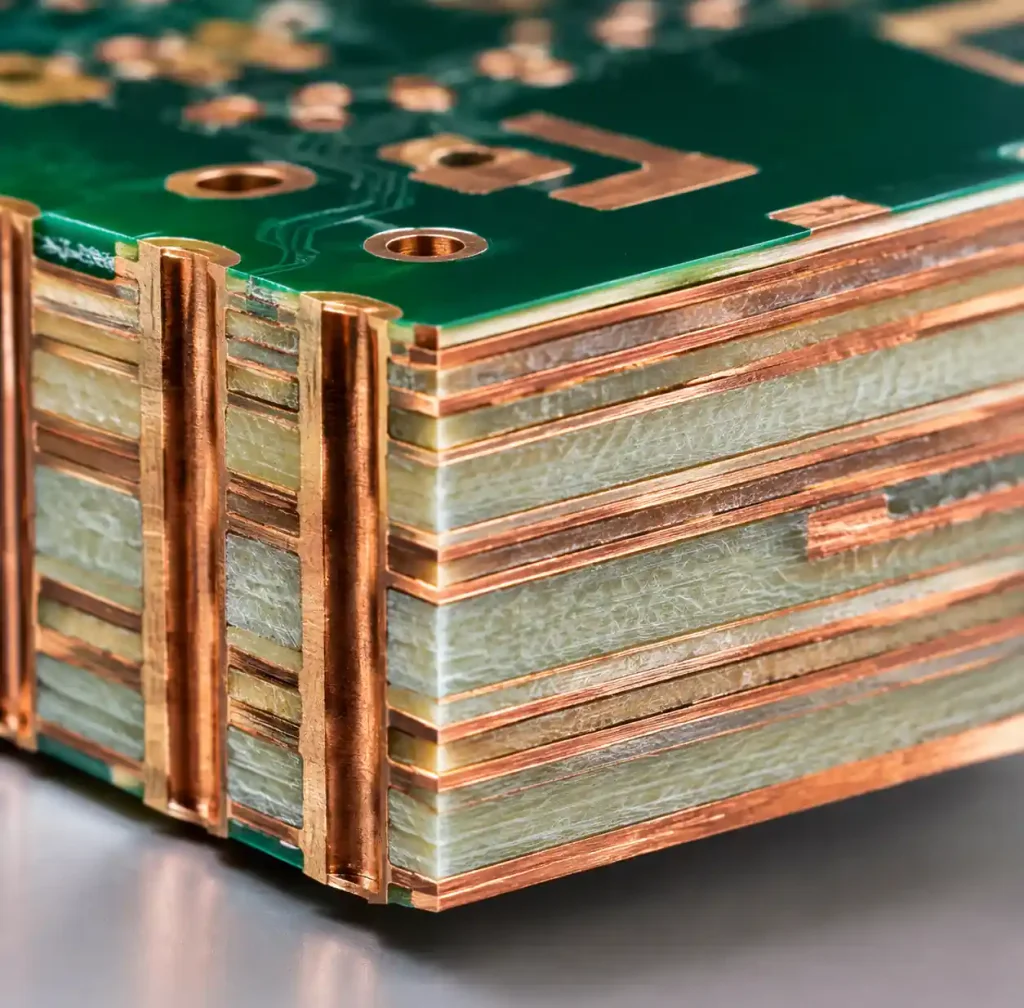
Multi-layer stackups for RF designs typically use 4-8 layers. A standard 4-layer RF stackup places signals on outer layers (microstrip) with continuous ground planes on layers 2 and 3, separated by power distribution. Six-layer stackups add dedicated power planes, while 8-layer designs provide stripline routing for sensitive signals between ground planes.
| Stackup Type | Layer Count | Signal Layers | Benefits | Applications |
|---|---|---|---|---|
| Simple microstrip | 2-4 layers | Top, bottom | Low cost, easy tuning | Prototypes, <5 GHz |
| Mixed | 4-6 layers | Microstrip + stripline | Shielding for digital | Transceivers, mixed-signal |
| Stripline | 6-8 layers | Internal only | Maximum isolation | Dense RF, mmWave |
| HDI | 8-14 layers | Multiple stripline | High integration | Phased arrays, 5G |
Via Design and Management
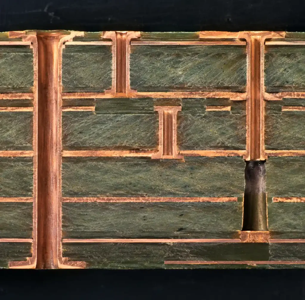
Vias introduce three parasitic effects that degrade RF performance: series inductance from the via barrel, shunt capacitance from the pad to ground planes, and stub resonance from unused via barrel length. A through-hole via on a 1.6mm board creates approximately 1nH inductance, forming a significant impedance discontinuity above 5 GHz.
Minimize via count on RF signal paths. When transitions between layers are unavoidable, use blind or buried vias instead of through-hole vias to reduce barrel length and eliminate stubs. A blind via from layer 1 to layer 3 on a 6-layer board has half the inductance of a through-hole via.
Via-in-pad technology places vias directly beneath component pads, eliminating the trace stub between pad and via. This technique is essential for BGA fan-out of mmWave ICs and antenna feeds above 20 GHz. Specify filled and capped vias—copper or epoxy fills the via barrel, then copper plating caps the top surface, creating a planar pad for reliable solder joints.
Backdrilling removes unused via stubs by drilling from the back side to mechanically remove the copper barrel beyond the last connected layer. For a via connecting layers 1 and 4 on an 8-layer board, backdrilling from layer 8 removes the stub from layer 5 to layer 8, eliminating stub resonance. Specify backdrill depth to stop 0.15-0.25mm past the last connection to avoid over-drilling into active layers.
Ground via stitching creates an RF ground mesh by placing grounded vias at regular intervals around RF sections and along transmission lines. Space ground vias at λ/10 intervals at your highest frequency—at 10 GHz in RO4003C, this means 2-3mm spacing. Ground via fencing forms a virtual wall preventing coupling between adjacent RF channels.
Layout Techniques for Signal Integrity
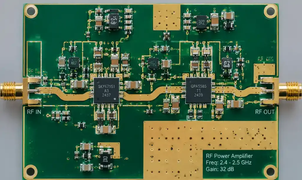
Keep RF signal paths as short as physically possible. Every millimeter of trace adds insertion loss and phase delay. Place RF components with minimal trace connections—position amplifiers close to filters, filters adjacent to mixers, with impedance-matched connections throughout the chain.
Avoid 90-degree corners in RF traces. Sharp corners create impedance discontinuities and radiate energy. Use chamfered corners (45-degree bends) or curved traces with radius at least 3 times the trace width. At millimeter-wave frequencies above 20 GHz, specify curved traces exclusively.
Separate RF and digital sections with grounded guard traces or ground plane gaps. High-speed digital signals generate broadband noise that couples into sensitive RF circuits through shared ground planes or electromagnetic radiation. When RF and digital circuits must coexist on the same board, place them on opposite sides with a solid ground plane between them, or use separate ground zones connected only at the power supply entry point.
Component orientation affects coupling and radiation. Orient amplifier input and output at 90 degrees or 180 degrees to maximize isolation and prevent feedback oscillation. Position sensitive low-noise amplifier inputs away from power amplifier outputs, with physical shielding (metal cans or ground via fences) between them.
Differential signaling provides natural common-mode noise rejection. RF differential pairs require tight coupling—space traces at 1-2 times trace width—and careful length matching within 0.1mm to maintain phase balance. Route differential pairs on the same layer without interruptions or reference plane changes.
Power Distribution and Decoupling
RF circuits demand extremely clean power with ripple below 1-10mV depending on circuit gain and noise figure. Switch-mode power supplies generate broadband noise requiring aggressive filtering before reaching RF stages.
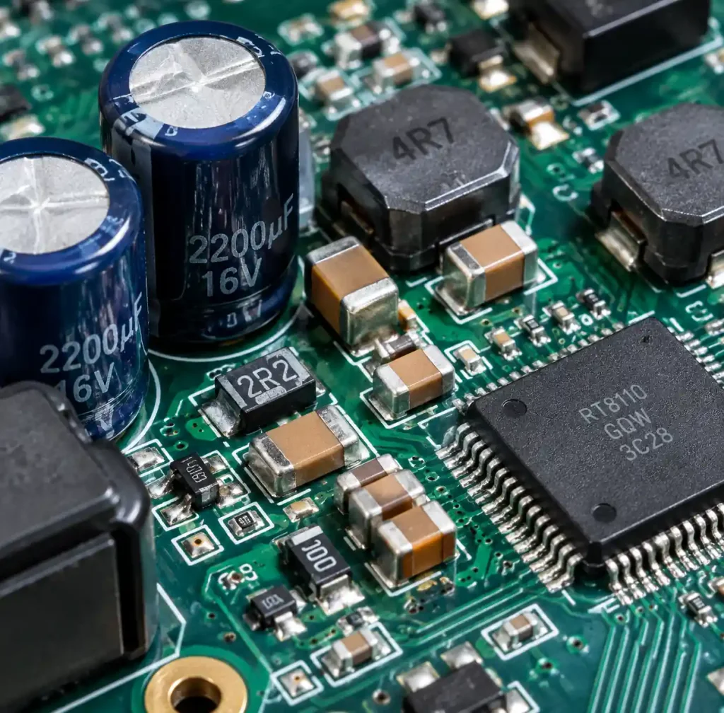
Design a multi-stage filtering network starting with bulk capacitors (10-100μF) at power entry, followed by ferrite beads (600-1000Ω at 100 MHz), then low-ESR ceramic capacitors (1-10μF) distributed across the board, and finally small ceramics (100nF, 10nF, 1nF) directly at each IC power pin.
Dedicate power planes or use wide power traces (>2mm) to reduce DC resistance and inductance. Separate analog and digital power domains, joining them only at a single point (star ground) to prevent digital noise from coupling into RF circuits. For sensitive circuits like voltage-controlled oscillators and low-noise amplifiers, implement local linear regulators providing additional isolation from system power noise.
Decoupling capacitor placement follows strict proximity rules. Place high-frequency decoupling (1-10nF) within 2mm of IC power pins using short, direct connections. Multiple vias to ground planes reduce inductance—use at least two vias per capacitor, one at each end. Avoid routing signals between IC power pins and their decoupling capacitors, as this introduces coupling paths.
Electromagnetic Shielding and Grounding
Ground planes serve three critical functions: signal return current paths, heat spreading, and electromagnetic shielding. Maintain continuous ground planes beneath all RF signal traces without gaps or splits. Return current flows directly beneath the signal trace—slots or gaps in the ground plane force current to detour, increasing loop inductance and degrading signal integrity.
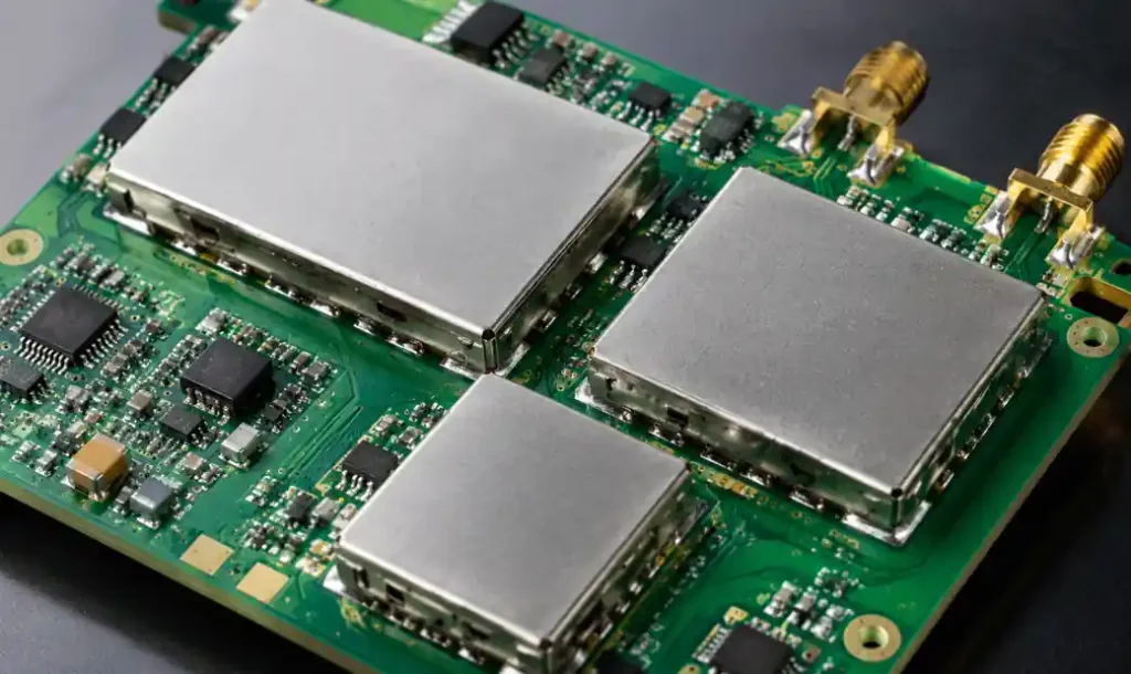
Metal shielding cans prevent electromagnetic coupling between circuit blocks and reduce radiation. Install shield cans over entire RF sections, connecting the can to PCB ground at multiple points around the perimeter. Specify cans with conductive gaskets or formed-in-place gaskets providing continuous electrical connection around the entire perimeter.
Shield can grounding requires careful via placement. Position grounded vias at 5-10mm intervals completely surrounding the shielded region, creating a virtual wall at the shield boundary. These vias must connect to the same ground plane referenced by RF traces inside the shield to prevent common-impedance coupling.
Implement RF gaskets at board-to-board or board-to-enclosure interfaces to maintain shielding continuity. Beryllium-copper or tin-plated steel fingers provide low-resistance connections while accommodating mechanical tolerances. Proper gasket compression requires 20-40% deflection—design mounting structures maintaining consistent gasket loading.
Manufacturing and Testing Considerations
Impedance Testing and Validation
All controlled impedance boards require test coupons—short transmission line segments fabricated on the production panel matching your design trace geometries. Manufacturers measure coupon impedance using time-domain reflectometry (TDR), adjusting trace widths on subsequent panels to achieve target impedance within tolerance.
Request impedance test reports documenting measured values for each coupon. Typical test resolution is ±2Ω for 50Ω traces. If measured impedance falls outside specification, root cause typically involves dielectric thickness variation, copper plating thickness, or etching process control.
DFM Guidelines
Maintain minimum trace width and spacing per your manufacturer’s RF capability—typically 4/4 mils (100/100μm) for high-frequency laminates. Tighter geometries are achievable but increase cost and yield loss. Avoid designing to minimum rules; use 5-6 mil traces and spacing unless electrical requirements demand otherwise.
Specify surface finish carefully. ENIG (electroless nickel immersion gold) provides flat, solderable surfaces but nickel creates slight magnetic loss above 10 GHz. Immersion silver or ENEPIG (electroless nickel electroless palladium immersion gold) offer better RF performance. For millimeter-wave designs above 30 GHz, specify smooth copper with thin surface finishes to minimize skin effect loss.
Order fabrication documentation per IPC-2581 or ODB++ formats including detailed stackup with material specifications, impedance requirements with test coupon locations, and via specifications (through-hole, blind, buried, filled, backdrilled). Clear documentation prevents misinterpretation and reduces fabrication delays.
Selecting an RF PCB Manufacturing Partner
When evaluating manufacturers for high-frequency PCBs, verify they stock Rogers, Taconic, or Isola RF laminates and have experience with hybrid stackups combining RF and FR-4 materials. Request impedance test data from previous production demonstrating they consistently achieve ±5% tolerance.
Andwin Circuits manufactures high-frequency PCBs from 1 GHz to 77 GHz with Rogers and Taconic materials in our IATF 16949 certified facility. We provide controlled impedance testing with TDR validation, support via-in-pad with copper fill, and offer quick-turn prototypes in 7-10 days. Our engineering team assists with stackup optimization and design for manufacturing reviews before fabrication.
For RF circuit designs requiring precision impedance control, see our guide on controlled impedance testing and TDR measurement. Learn more about material selection in our Rogers high-frequency board guide.
FAQ
What is the difference between high-frequency and high-speed PCB design?
High-frequency design addresses RF and microwave circuits from 500 MHz to 77+ GHz where signals propagate as electromagnetic waves requiring impedance-matched transmission lines, low-loss materials, and careful EM coupling control. High-speed digital design handles fast edges and rise times (typically <1ns) but operates at lower fundamental frequencies, focusing on signal integrity, timing, and crosstalk rather than impedance matching and insertion loss.
Can I use FR-4 for RF designs below 5 GHz?
High-quality FR-4 with Dk=4.2-4.4 and Df<0.010 works for prototype and low-cost RF designs below 3-5 GHz if you accept higher insertion loss (typically +0.5-1.0dB vs Rogers materials) and tighter fabrication tolerances. Production designs benefit from RF laminates providing better consistency and lower loss.
How do I calculate trace width for 50-ohm impedance?
Use field solver software (many manufacturers provide free calculators) inputting your material Dk, dielectric thickness, copper thickness, and transmission line type (microstrip or stripline). Typical 50Ω microstrip on 0.5mm thick RO4003C requires 1.0-1.2mm trace width. Verify calculations with test coupons from your manufacturer.
What is the maximum frequency for standard PCB fabrication?
Standard PCB processes reliably produce boards for frequencies up to 20-30 GHz using Rogers materials and controlled impedance design. Millimeter-wave applications from 30-77 GHz require tighter process controls, smoother copper, and specialized design techniques including cavity-backed antennas and substrate-integrated waveguides.
Why do vias matter in RF design?
Vias introduce parasitic inductance (approximately 1nH per millimeter of via length) and capacitance that create impedance discontinuities degrading insertion loss and return loss. Via stubs create resonances at specific frequencies causing sharp dips in performance. Minimize via count, use blind/buried vias, and implement backdrilling for frequencies above 5 GHz.
Conclusion
High-frequency PCB design requires attention to material properties, controlled impedance transmission lines, via management, and electromagnetic shielding. Success depends on selecting materials with stable Dk and low Df, implementing proper stackup and impedance control, minimizing parasitics through careful via design, and maintaining ground plane integrity throughout the layout.
Andwin Circuits delivers high-frequency PCB solutions from prototypes to production volumes using Rogers RO4000/RO3000 series and Taconic RF materials with controlled impedance testing and quick turnaround. Our engineering support includes stackup design, DFM review, and impedance simulation. Contact us today for your RF and microwave PCB manufacturing needs with competitive factory-direct pricing.