
Controlled Impedance Testing: TDR Measurement and Coupon Design
High-speed digital designs fail predictably when impedance mismatches distort signal edges. TDR testing catches these manufacturing variations before boards ship, but test accuracy depends entirely on coupon design and measurement procedure. A 5-ohm impedance error at 1 GHz creates 200 mV noise on a 3.3V signal—enough to corrupt data in DDR4, PCIe, or USB 3.2 interfaces.
What Is Controlled Impedance Testing?
Controlled impedance testing verifies that fabricated PCB traces match design targets within specified tolerances. The process measures characteristic impedance (Z₀) of transmission line structures using time-domain reflectometry (TDR), comparing actual values against design specifications.
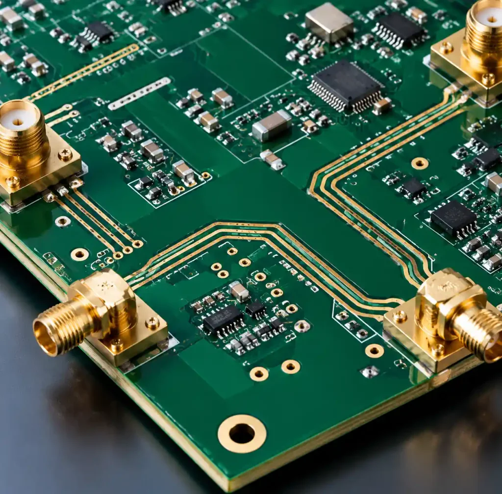
You need controlled impedance verification when signal rise times drop below 1 nanosecond or frequencies exceed 50 MHz. At these speeds, traces behave as transmission lines where impedance mismatches cause reflections, ringing, and signal integrity failures.
According to IPC-2141, typical tolerance is ±10% (±5Ω for 50Ω targets, ±10Ω for 100Ω differential pairs). High-reliability applications like medical devices and aerospace systems often require ±7% or tighter.
Time Domain Reflectometry (TDR) Fundamentals
TDR instruments launch a fast voltage step into the trace under test and measure reflected signals. When the step encounters an impedance change, a portion reflects back. The reflected waveform amplitude reveals impedance magnitude; timing indicates discontinuity location.
The measurement relies on transmission line theory. A 50Ω TDR instrument connected to a 50Ω trace sees no reflection. A 60Ω trace reflects positive voltage (higher impedance); a 40Ω trace reflects negative voltage (lower impedance).
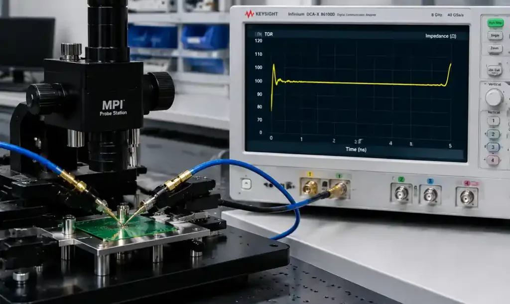
Modern TDR equipment provides sub-100 ps rise times, resolving impedance variations along traces as short as 3-5 mm. Professional TDR systems from Tektronix, Keysight, and Polar Instruments achieve ±1-2Ω measurement uncertainty after proper calibration.
Impedance Coupon Design Requirements
Impedance coupons are test traces fabricated on the manufacturing panel alongside production boards. They represent critical transmission line stackups, allowing destructive testing without sacrificing functional boards.
Effective coupon design requires matching the production stackup exactly—same copper weight, dielectric thickness, trace width, and distance to reference planes. Any deviation between coupon and production geometry invalidates the measurement.
| Coupon Design Parameter | Minimum Requirement | Recommended Practice |
|---|---|---|
| Trace Length | 100 mm (4 inches) | 150-200 mm for cleaner measurement |
| Ground Plane Clearance | 10× trace width | 15-20× trace width to avoid edge effects |
| Launch Pad Size | 1.5 mm diameter | SMA footprint compatible (2.5-3 mm) |
| Trace Spacing | 3× trace width | 5× trace width for isolation |
| Number of Traces per Stackup | 1 (minimum) | 2-3 for statistical validation |
You should place coupons in the panel border area where fabrication conditions match the production board center. Corner locations experience different etch rates and lamination pressure, producing non-representative results.
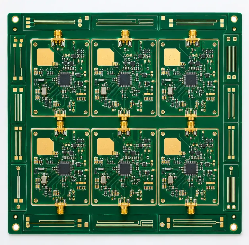
For multilayer HDI designs, include separate coupons for each controlled impedance layer. A 10-layer board with 50Ω microstrip on L1, 100Ω stripline on L4/L5, and 90Ω differential pairs on L2 requires minimum three coupon types.
Coupon Trace Length and Geometry
TDR measurements need sufficient trace length to separate launch discontinuity reflections from actual trace impedance. Short coupons produce overlapping waveforms that obscure true values.
The minimum functional length is 100 mm, providing approximately 650 ps propagation delay in FR4. This separates reflections by 1.3 ns—adequate for rise times above 200 ps.
Production coupons between 150-200 mm offer better measurement windows, improving accuracy to ±1-2Ω versus ±3-4Ω for 100 mm coupons.
Trace width must match production design within ±5 μm. A 100 μm width variation changes 50Ω microstrip impedance by 3-5Ω. Fabrication houses achieving ±25 μm trace control deliver consistent impedance.
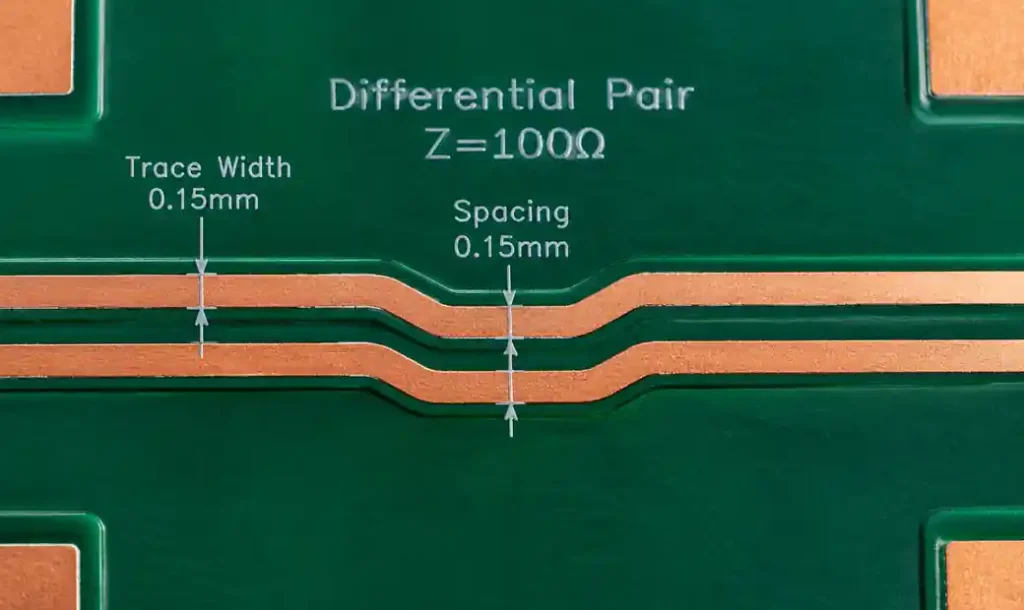
Differential pair coupons require maintaining both trace width and spacing tolerances. A 100Ω differential pair with 125 μm traces and spacing shifts to 95Ω if spacing opens to 175 μm during etching.
TDR Measurement Procedure and Setup
Proper TDR measurement starts with instrument calibration. Connect calibration standards (open, short, 50Ω load) to establish reference impedance. Temperature-stable precision loads prevent drift during multi-hour test sessions.
Position SMA connectors or probe tips on coupon launch pads with controlled contact force. Excessive pressure deforms pads; insufficient contact creates intermittent connections. Spring-loaded fixtures maintain 100-200 grams force per probe, ensuring repeatable measurements.
| Measurement Step | Critical Parameter | Acceptable Range |
|---|---|---|
| Calibration Frequency | Before each test session | Every 2-4 hours minimum |
| Rise Time | Match signal speeds | 35 ps for 10 GHz, 100 ps for 3 GHz |
| Sampling Points | Trace uniformity check | Minimum 3 locations per 100 mm |
| Averaging | Reduce noise floor | 16-64 waveforms |
| Cursor Placement | Exclude launch/termination | Center 50-70% of trace length |
The TDR waveform displays impedance versus distance. Place measurement cursors in the flat central region, avoiding the initial 10-20 mm (launch transition) and final 10-20 mm (termination). Calculate average impedance from this region for comparison against targets.
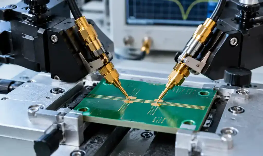
Temperature affects measurements. FR4 dielectric constant decreases 0.02-0.03 per 10°C temperature rise, changing 50Ω traces by 0.5-1Ω. Record ambient temperature during testing for correlation with design calculations assuming 25°C baseline.
For high-frequency telecom applications, TDR provides time-domain characterization while VNA S-parameter testing validates frequency-domain performance. Both methods together reveal manufacturing quality.
Interpreting TDR Waveforms and Identifying Issues
A clean TDR trace shows a flat impedance region between launch and termination discontinuities. This indicates uniform trace geometry and consistent dielectric properties.
Positive impedance spikes indicate width reductions or increased dielectric thickness. A sudden 10Ω rise over 5 mm suggests localized over-etching or lamination voids. Negative impedance dips reveal width increases or reduced dielectric thickness.
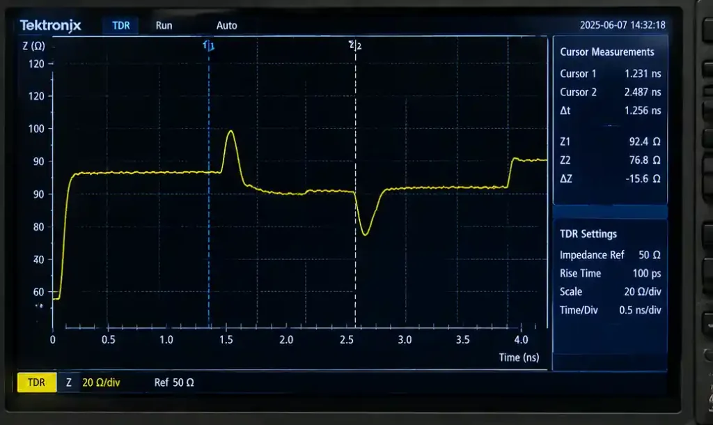
Gradual impedance slopes indicate systematic fabrication drift—progressive etching variations or dielectric thickness gradients across the panel. Slopes exceeding 0.5Ω per 10 mm signal process control problems.
Multiple periodic variations suggest registration issues between layers. When outer traces and inner reference planes misalign during lamination, the effective dielectric thickness oscillates, creating repetitive impedance modulation.
Tolerance Analysis and Pass/Fail Criteria
Manufacturing tolerance stackup determines achievable impedance control. Copper thickness varies ±10-15% (0.5 oz ±0.07 oz), dielectric thickness ±10% typical (4 mil ±0.4 mil), and trace width ±1-2 mils after etching.
These variations combine to create ±3-5Ω impedance spread on 50Ω targets under typical 4-layer stackup configurations. Tighter control requires specifying closer tolerances, increasing fabrication cost 15-30%.
| Tolerance Grade | Impedance Accuracy | Typical Applications | Cost Impact |
|---|---|---|---|
| Standard (±10%) | ±5Ω on 50Ω | Consumer electronics, IoT | Baseline |
| Controlled (±7%) | ±3.5Ω on 50Ω | Automotive, industrial | +15-20% |
| Precision (±5%) | ±2.5Ω on 50Ω | Telecom, medical, aerospace | +25-35% |
Pass/fail decisions depend on application requirements. USB 2.0 tolerates ±15% (90Ω ±13.5Ω differential). PCIe Gen 4 requires ±10% (85Ω ±8.5Ω). SerDes interfaces above 25 Gbps often specify ±7% for adequate eye margin.
Document all measurements in test reports including waveform screenshots, cursor positions, temperature, and equipment calibration status. IPC-TM-650 method 2.5.5.7 defines standard reporting format for impedance testing.
Troubleshooting Common Impedance Failures
When measurements fall outside tolerance, systematic troubleshooting identifies root causes. Start by verifying coupon design matches production stackup—incorrect dielectric thickness assumptions cause most impedance failures.
Check trace width under microscope. Actual copper width after etching often differs from Gerber artwork by 0.5-2 mils. Adjust etch compensation and remeasure. Dielectric constant variations between material lots shift impedance 2-4Ω.
Copper plating thickness affects microstrip impedance strongly. Additional 0.5 oz plating on outer layers reduces trace height-to-width ratio, lowering impedance 3-5Ω. Verify final copper weight matches specifications through cross-sectional analysis.
Statistical Process Control for Production
High-volume production requires statistical monitoring. Sample plans per IPC-2141 specify testing frequency based on lot size and process capability.
Typical automotive programs test 2-5 coupons per panel for process monitoring. Each measurement contributes to control charts tracking impedance mean and standard deviation over time.
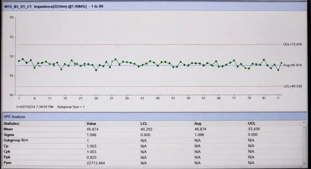
Control limits set at ±3 sigma detect process shifts before out-of-tolerance boards ship. Process capability index (Cpk) quantifies manufacturing consistency. Cpk > 1.33 indicates capable processes meeting ±10% tolerance with margin.
For critical applications, implement automated TDR testing integrated with panel handling systems for complete traceability with medical and automotive compliance.
Design for Testability
Optimize designs to simplify impedance verification. Place test points on high-speed nets near connectors, allowing correlation between coupon measurements and in-circuit TDR probing.
Route critical impedance-controlled traces without vias when possible. Each via introduces 5-10 mm stub length creating impedance discontinuity. Minimizing vias improves signal integrity and simplifies coupon representation.
Specify impedance requirements clearly on fabrication drawings: target impedance, tolerance, test method (TDR per IPC-TM-650 2.5.5.7), and acceptance criteria. Work with fabrication houses to validate stackups using field solver software before production.
FAQ
Q: What is the minimum trace length needed for accurate TDR testing?
A: 100 mm minimum, but 150-200 mm recommended. Shorter traces produce overlapping reflections that obscure true impedance measurement.
Q: How does temperature affect impedance measurements?
A: FR4 dielectric constant decreases 0.02-0.03 per 10°C rise, changing 50Ω impedance by 0.5-1Ω. Perform measurements at controlled room temperature (23±2°C).
Q: Can one coupon represent multiple impedance values?
A: No. Each unique stackup configuration requires a separate coupon. A board with 50Ω microstrip, 100Ω stripline, and 90Ω differential pairs needs three distinct coupon types.
Q: What causes periodic impedance variations in TDR waveforms?
A: Registration misalignment between copper layers during lamination. When outer traces and inner reference planes shift position, effective dielectric thickness varies periodically.
Q: How often should TDR equipment be calibrated?
A: Before each test session minimum, every 2-4 hours for extended testing. Temperature changes, probe wear, and cable movement affect calibration accuracy.
Q: What impedance tolerance applies to high-speed digital designs?
A: Standard tolerance is ±10% per IPC-2141. USB and Ethernet typically specify ±10-15%. PCIe Gen 4/5 requires ±10%. SerDes above 25 Gbps often needs ±7% or tighter.
Conclusion
Controlled impedance testing validates that manufactured PCBs meet high-speed signal integrity requirements. TDR measurement provides accurate characterization when coupons accurately represent production stackups and procedures follow calibrated measurement protocols.
Effective testing programs combine proper coupon design—matching production geometry with adequate trace length and isolation—with systematic TDR procedures including calibration, cursor placement, and environmental control. Statistical process control transforms individual measurements into process capability data that prevents failures before they occur.
Manufacturing capability determines achievable tolerances. Standard ±10% tolerance suits most applications while precision ±5% control serves aerospace and high-speed SerDes designs requiring superior signal integrity.
Andwin Circuits provides controlled impedance PCB manufacturing up to 50 layers with comprehensive TDR testing and documentation. Our ISO 9001 and IATF 16949 certified facility delivers impedance-controlled boards for telecommunications, automotive, medical, and high-speed digital applications. Contact us for impedance testing specifications, stackup design support, and fast turnaround on your high-speed PCB requirements.