How to design a PCB
1. Preliminary preparation
Including preparation of component libraries and schematics. Before conducting PCB design, you must first prepare the schematic SCH component library and PCB component packaging library.
The PCB component packaging library is best established by engineers based on the standard size data of the selected devices. In principle, the PC component package library should be established first, and then the schematic SCH component library should be established.
The requirements for the PCB component package library are relatively high, which directly affects the installation of the PCB. The requirements for the schematic SCH component library are relatively loose, but attention should be paid to defining the pin attributes and the corresponding relationship with the PCB component package library.
2. PCB structure design
According to the determined circuit board size and various mechanical positioning, draw the PCB board frame in the PCB design environment, and place the required connectors, buttons/switches, screw holes, assembly holes, etc. according to the positioning requirements.
Fully consider and determine the wiring area and non-wiring area (such as how much area around the screw hole belongs to the non-wiring area).
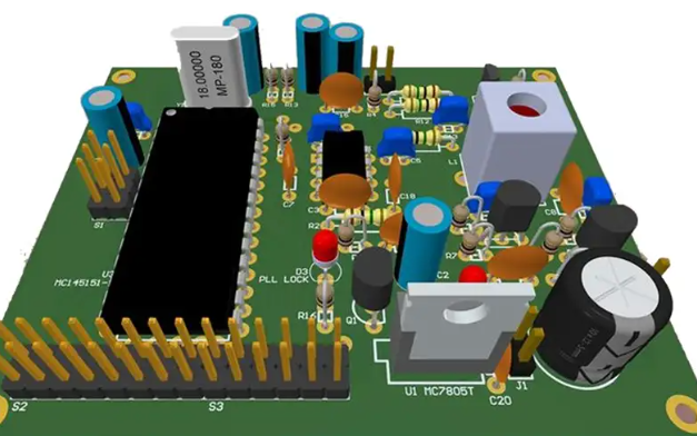
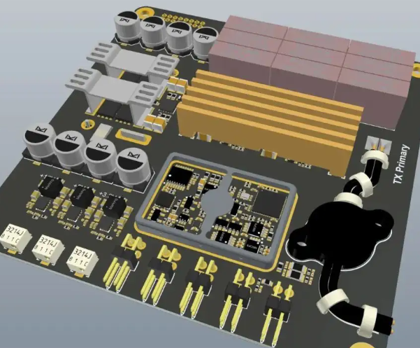
3. PCB layout design
Layout design is to place devices in the PCB board frame according to the design requirements.
Generate the netlist in the schematic tool (Design→Create Netlist), and then import the netlist in the PCB software (Design→Import Netlist). After the network table is successfully imported, it will exist in the software background.
All devices can be called out through the Placement operation. There are flying wires between each pin to prompt connection. At this time, the device layout design can be carried out. PCB layout design is the first important process in the entire PCB design process.
The more complex the PCB board, the more the quality of the layout will directly affect the difficulty of later wiring. Layout design relies on the circuit board designer’s basic circuit skills and design experience, and has higher-level requirements for circuit board designers. Junior circuit board designers have little experience and are suitable for small module layout design or less difficult PCB layout design tasks for the entire board.
PCB wiring design PCB wiring design is the process with the largest workload in the entire PCB design, which directly affects the performance of the PCB board.
In the PCB design process, there are generally three realms of wiring: first, layout, which is the most basic entry requirement for PCB design; second, satisfaction of electrical performance, which is the standard for measuring whether a PCB board is qualified. After passing through, carefully adjust the wiring to achieve the best electrical performance; again, neat and beautiful wiring, messy wiring, even if the electrical performance passes, will bring great inconvenience to later board modification optimization, testing and maintenance, and neat wiring is required Uniform, not criss-crossed and unorganized.
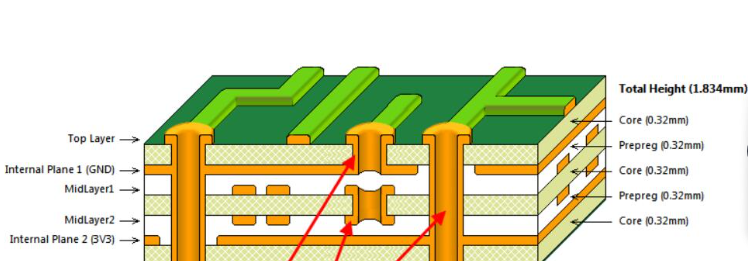
Wiring optimization and silk screen placement “PCB design is not the best, only better”, “PCB design is an art of defects”, this is mainly because PCB design must meet the design requirements of all aspects of hardware, and individual requirements may vary. It’s conflicting, and you can’t have your cake and eat it too. For example, a PCB design project needs to be designed as a 6-layer board after evaluation by the circuit board designer.
However, due to cost considerations, the product hardware must be designed as a 4-layer board. In this case, the signal shielding ground layer can only be sacrificed, resulting in adjacent wiring. Signal crosstalk between layers increases and signal quality decreases. A general design rule of thumb is that optimizing wiring takes twice as long as initial wiring.
After PCB wiring optimization is completed, post-processing is required. The first thing to deal with is the silk screen logo on the PCB board. During design, the bottom silk screen characters need to be mirrored to avoid confusion with the top silk screen.
Network DRC inspection and structural inspection Quality control is an important part of the PCB design process. General quality control methods include: design self-inspection, design mutual inspection, expert review meetings, special inspections, etc. Schematic diagram and structural element diagram are the most basic design requirements. Network DRC check and structural inspection are to confirm that the PCB design meets the two input conditions of schematic netlist and structural element diagram respectively. Generally, circuit board designers will have their own accumulated design quality inspection Checklist, in which the items are partly derived from the company or department’s specifications, and the other part are derived from their own experience summaries. Special inspections include Valor inspection and DFM inspection of the design. These two parts focus on the back-end processing of light drawing files for PCB design output.
Conclusion. PCB board making. Before the PCB is officially processed and made, the circuit board designer needs to communicate with the PE of the PCB supplier factory and answer the manufacturer’s confirmation questions about PCB board processing. This includes but is not limited to: PCB board model selection, line layer line width and line spacing adjustment, impedance control adjustment, PCB stacking thickness adjustment, surface treatment processing technology, aperture tolerance control and delivery standards, etc. Our company will provide special customization services. If you have special customization needs for PCB boards, you can contact us. including Heavy copper PCB、Copper core PCB、Metal core PCB、Ceramic PCB、Radio frequency PCB、High speed PCB