
IC Test Board Fixturing: Pogo Pin and Probe Card Design
IC test board fixturing accounts for 15-25% of semiconductor test costs, with probe contact reliability directly affecting yield measurement accuracy. Poor fixturing design causes false failures, extended test times, and costly product escapes in volume production.
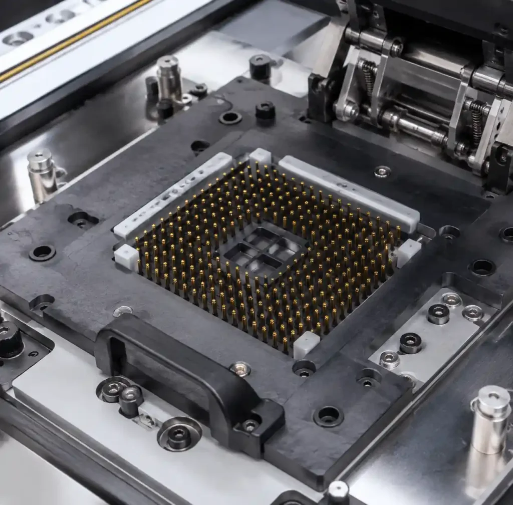
This guide covers pogo pin selection, probe card design for wafer testing, contact resistance minimization, force uniformity, alignment features, and DUT socket integration for reliable IC testing connections.
What is IC Test Board Fixturing?
IC test board fixturing is the mechanical and electrical interface connecting a Device Under Test (DUT) to Automatic Test Equipment (ATE) through spring-loaded probes (pogo pins), probe cards, or socket contactors. This fixturing provides temporary electrical contact to IC pins or wafer bond pads for parametric testing and functional verification.
Test fixturing must deliver stable contact resistance (<50mΩ), controlled contact force (25-100 grams-force), precise alignment (±25μm for wafer probes), and durability exceeding 100,000 cycles. The system includes probe interface, alignment hardware, and signal conditioning to ensure measurement repeatability.
Pogo Pin Selection Criteria
Contact Force and Stroke Requirements
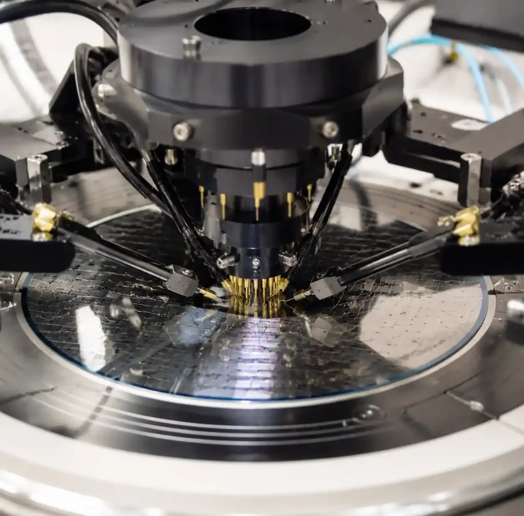
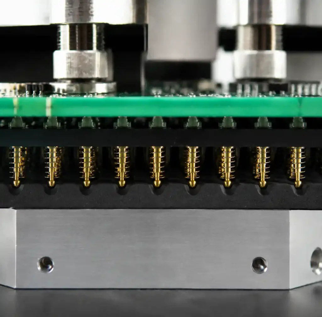
Pogo pin contact force determines connection reliability. Standard applications require 40-60 grams-force per pin. Higher force (80-100gf) suits high-current pins or oxidized pads, while delicate die contacts use 15-25gf to prevent pad damage.
Specify pogo pins with 0.5-2.0mm stroke length depending on planarity tolerance. A 6-layer PCB with ±0.1mm thickness variation requires minimum 1.0mm stroke. According to industry specifications, pogo pins maintain <10% force variation over the middle 50% of stroke travel.
| Pogo Pin Type | Contact Force | Stroke | Current | Application |
|---|---|---|---|---|
| Standard | 40-60 gf | 1.0-1.5mm | 1-3A | Digital IC testing |
| High-Current | 80-120 gf | 0.8-1.2mm | 5-10A | Power management IC |
| Fine-Pitch | 15-30 gf | 0.5-1.0mm | 0.5-1A | Wafer probing |
| RF | 25-50 gf | 0.8-1.5mm | 1-2A | Up to 50 GHz testing |
Contact Resistance and Plating
Contact resistance below 50mΩ ensures accurate measurement. Gold plating over nickel provides 10-30mΩ resistance. Recent research shows 5μm gold plating maintains <0.07dB insertion loss at 10 GHz with resistance below 20mΩ after 50,000 cycles.
For high-current applications exceeding 3A, specify beryllium-copper spring elements with 10-15μm gold over 1.5-3μm nickel underplate. Tin or palladium plating is unsuitable because oxide formation increases resistance above 100mΩ after 10,000 cycles.
Probe Card Design for Wafer Testing
Probe Card Technologies
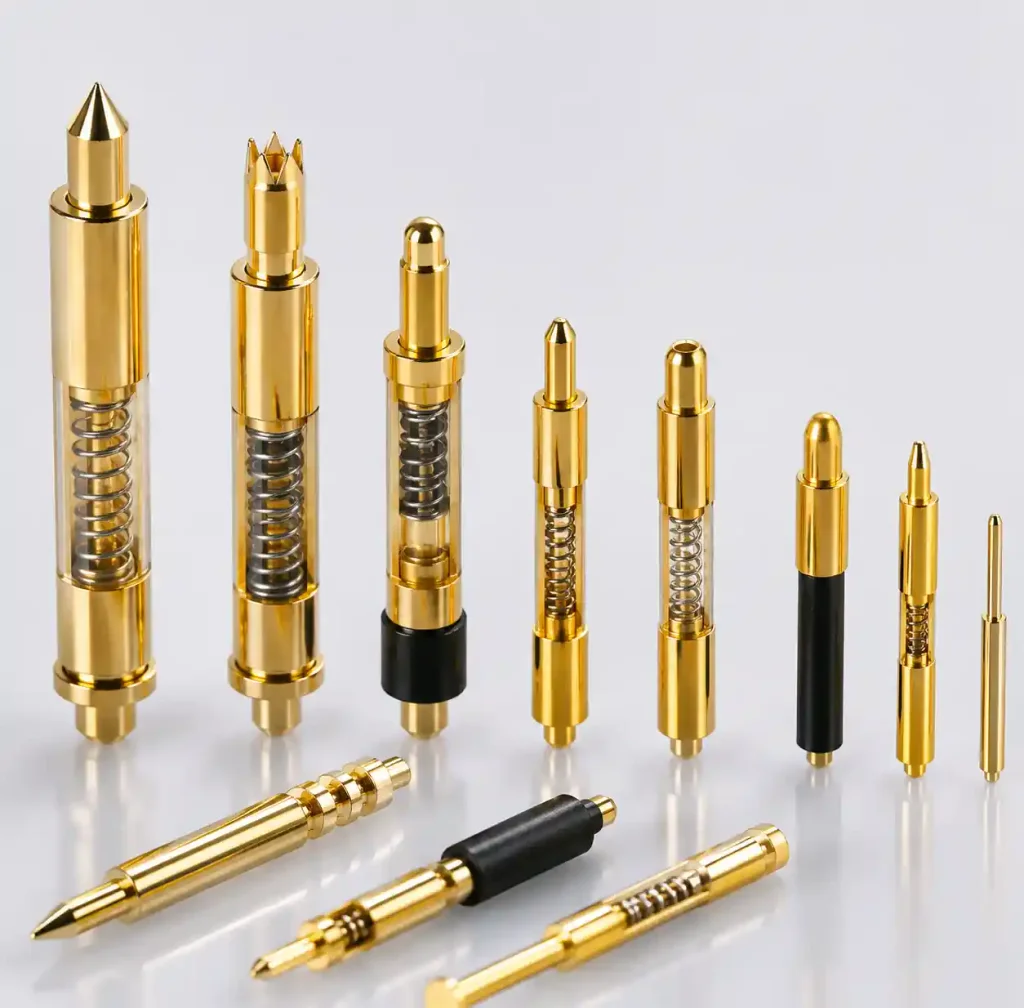
Wafer-level probe cards connect ATE to IC die on silicon wafers before dicing. Vertical MEMS probe cards enable 50-100μm pitch with 2-10A per contact and single-digit nanohenry inductance for advanced nodes below 7nm. These replace cantilever designs that cannot achieve required density.
Cantilever probe cards suit coarser pitches (150-400μm) with scrub action of 15-50μm to penetrate oxide. Vertical MEMS probes contact perpendicular to wafer with <7% scrub ratio per 2025 SW Test data, reducing pad damage and enabling finer pitch.
Alignment and Thermal Compensation
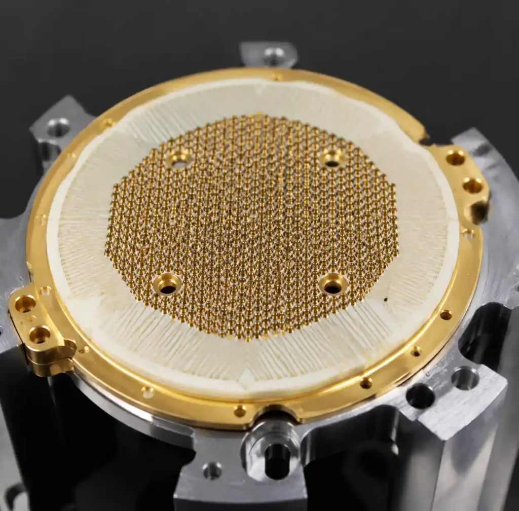
Probe-to-pad alignment requires ±25μm accuracy at -40°C to +150°C. Thermal expansion requires CTE-matched materials. Use ceramic substrates (alumina or LTCC with CTE 6-7 ppm/°C) matching silicon wafer CTE (2.6 ppm/°C) within 5 ppm/°C to prevent misalignment during temperature testing.
| Probe Type | Pitch | Scrub | Current | Lifespan | Cost |
|---|---|---|---|---|---|
| Cantilever | 150-400μm | 15-50μm | 0.5-2A | 50k-100k | Low |
| Vertical MEMS | 50-100μm | <5μm | 2-10A | 500k-1M | High |
| Cobra/Blade | 100-200μm | 20-40μm | 1-5A | 100k-200k | Medium |
Contact Resistance Minimization
Surface Preparation
DUT pad oxidation increases contact resistance from 25mΩ to >500mΩ within months. ENIG provides 0.05-0.15μm gold over 3-5μm nickel maintaining <50mΩ for 12-24 months. OSP costs 40-60% less but oxidizes within 3-6 months.
Implement probe cleaning every 1000-2000 touchdowns using isopropyl alcohol. Industry experience shows regular cleaning maintains resistance below 30mΩ compared to >100mΩ for uncleaned probes after 10,000 contacts.
Force Distribution Control
Uniform contact force requires 30-50% overdrive of total stroke. For 1.0mm stroke pins, design 0.3-0.5mm overdrive. Implement polyurethane backing (50-70 Shore A) that compresses 10-20% under load, reducing force variation from ±20% to ±10% across 100+ pin arrays.
Probe Card PCB Design
Signal Integrity and Stackup
Probe cards require 6-20 layers separating signal from ground planes. A 12-layer stackup uses Signal/Ground/Signal/Power configuration with 0.1mm trace width and spacing on outer layers.
Reference our IC test board high-frequency probing guide for impedance control. Specify 50Ω single-ended or 100Ω differential ±10% per IPC-2141. Ground planes must cover >90% providing <2nH inductance per via.
Kelvin Sensing
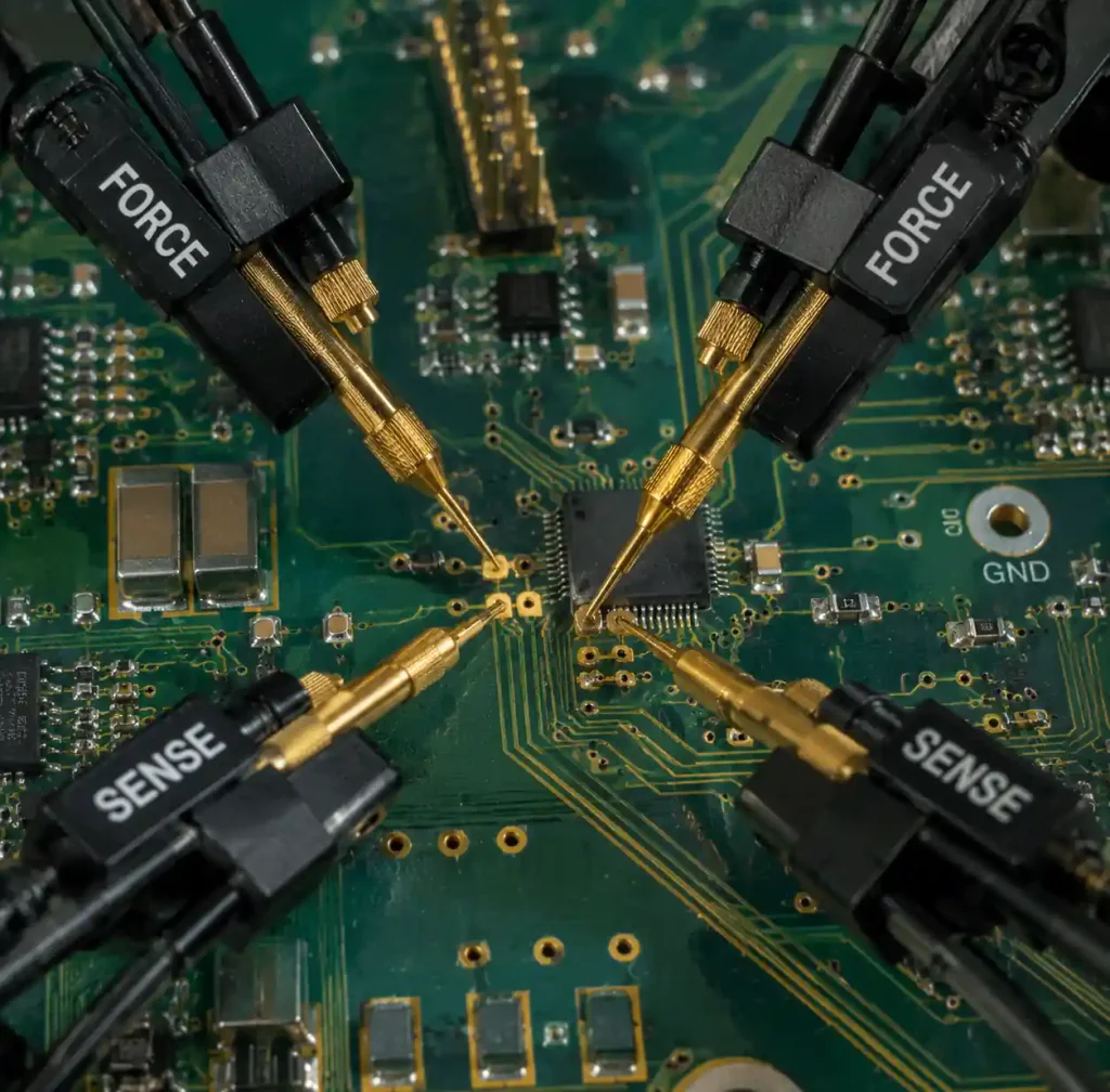
Four-wire Kelvin sensing eliminates probe contact resistance from measurement. Each DUT pin requires two contacts: force carries test current, sense measures voltage with <1μA current eliminating voltage drop from contact resistance.
Design Kelvin pairs with 200-500μm spacing to minimize inductance. Route as twisted or parallel differential pairs with <0.5mm separation. Proper implementation achieves ±0.1mV accuracy compared to ±2-5mV for two-wire measurements with 50mΩ at 100mA.
DUT Socket Integration
Socket Contact Technologies
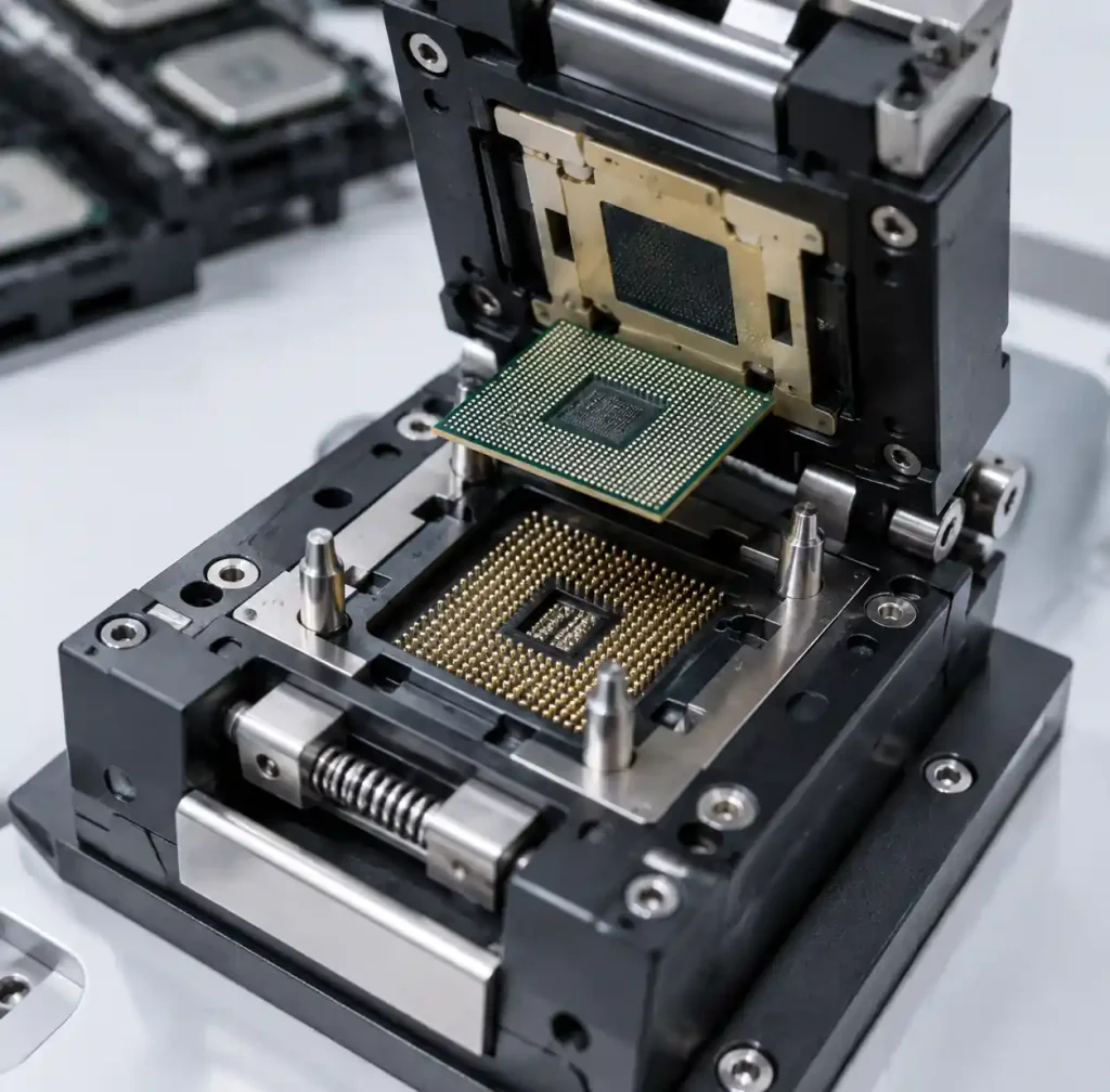
DUT sockets provide temporary connections for package testing. Land Grid Array (LGA) sockets use pogo pin contactors achieving <30mΩ resistance with 100,000+ cycles. Ball Grid Array (BGA) sockets employ compliant pin or elastomer contacts providing 50-80mΩ with 5,000-10,000 cycle lifespan.
Specify socket pitch matching IC package. A 0.5mm pitch BGA requires fine-pitch elastomer or cantilever contacts. For QFN packages with exposed thermal pads, integrate thermal contact pins carrying 5-10A for power delivery and heat extraction during 125-150°C burn-in testing.
Alignment Mechanisms
Socket alignment uses precision-machined features maintaining ±50μm accuracy. Clamping applies uniform force preventing tilt. For 15×15mm packages, distribute 200-400gf through four corner clamps or pneumatic actuators providing 50-100gf per contact.
Design contactors with 0.3-0.5mm Z-axis compliance allowing individual pins to follow package warpage (50-150μm across 20mm diagonal) while maintaining contact force.
High-Frequency Probe Design
RF and Millimeter-Wave Probing
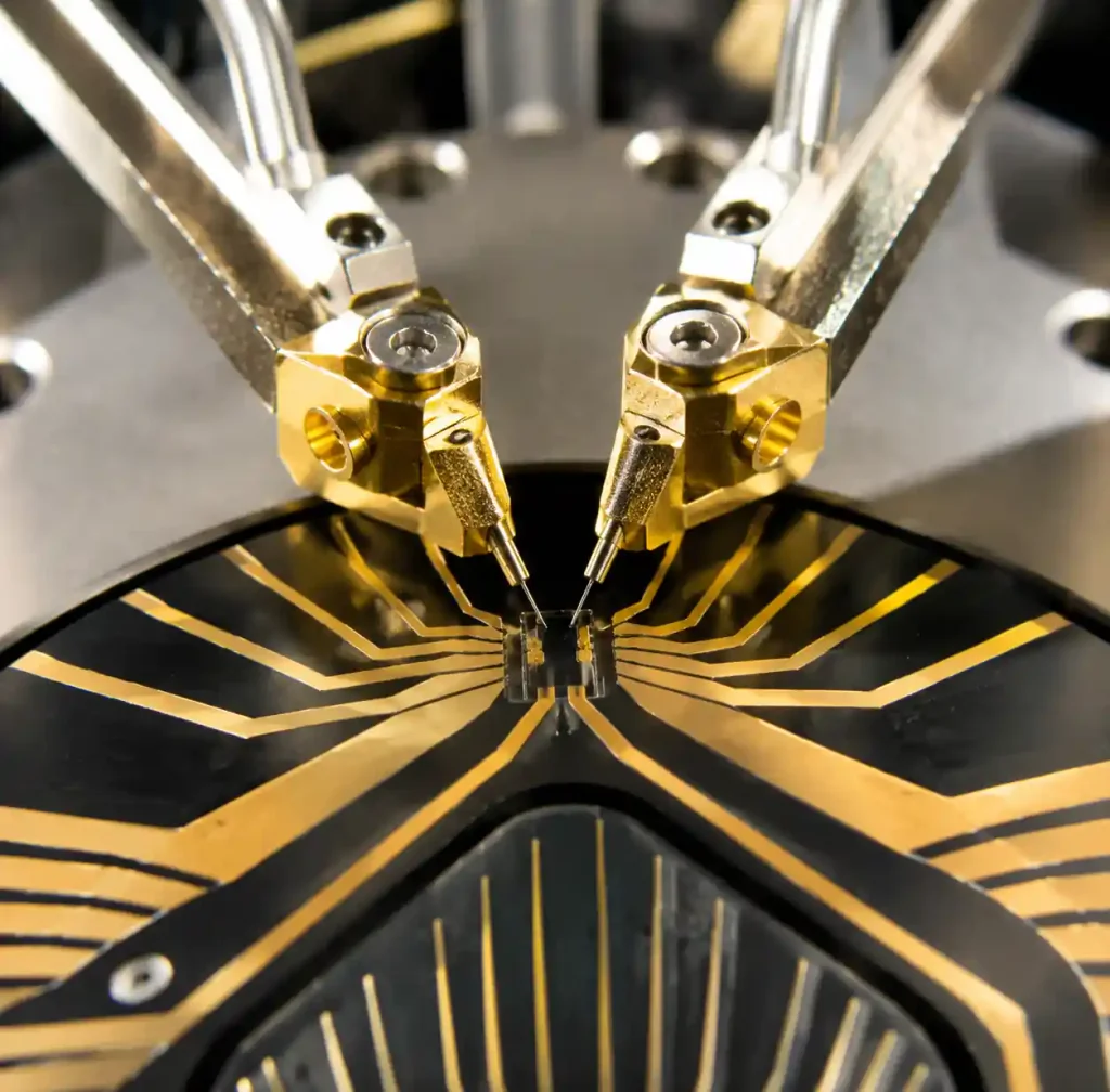
RF IC testing above 10 GHz requires coplanar waveguide (CPW) designs. 50 GHz pogo pin research shows metallic socket designs eliminate signal leakage. Ground-signal-ground (GSG) configuration with 150μm pitch maintains 50Ω impedance and <1dB insertion loss at 50 GHz.
For millimeter-wave testing above 30 GHz, use 10-25μm radius tips contacting 50×50μm pads with <15μm scrub. Probe launches require gradual taper from 500μm barrel to 25μm tip over 2-3mm length reducing reflection below -15dB.
Crosstalk Prevention
High-density arrays exhibit -30dB crosstalk at 1 GHz increasing to -15dB at 10 GHz without shielding for <500μm spacing. Implement ground guards between signals or GSG/GSSG patterns. RF testing shows ground pins connected to plane within 200μm reduce crosstalk below -40dB at 10 GHz.
Fixture Maintenance Strategies
Contact Resistance Monitoring
Probe resistance increases 50-200% over lifetime due to wear and contamination. Monitor each probe at 1mA every 5,000-10,000 touchdowns. Replace cards when average resistance exceeds 50mΩ or variation exceeds 2:1 ratio.
Track touchdown count per position because edge probes contact first and wear faster. Replace outer 20% at 50,000 touchdowns while center probes last 100,000+ touchdowns, reducing cost versus full replacement.
Cleaning Protocols
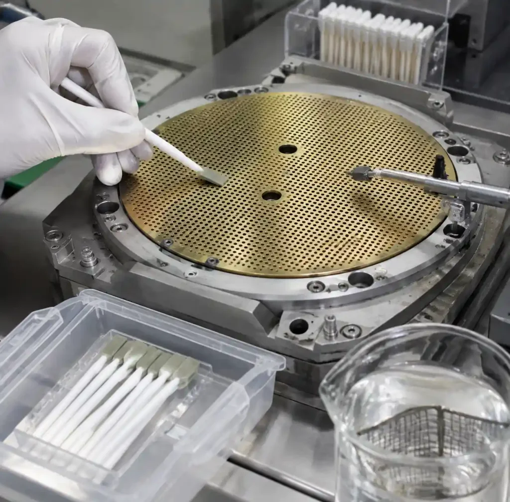
Clean probes every 1,000-2,000 touchdowns maintaining resistance and extending life by 2-3×. Use abrasive rubber pads (Shore A 60-75) with 20-30 cycles, then wipe with isopropyl alcohol removing particles.
For high-value MEMS cards ($20,000-100,000), implement ultrasonic cleaning at 40 kHz for 60-90 seconds. Research shows this extends life beyond 500,000 touchdowns for gold-plated vertical MEMS probes.
Selecting Test Board Manufacturers
When choosing a manufacturer, verify high-density interconnect and impedance design experience. The manufacturer should demonstrate probe card PCB capabilities including microvias (0.1mm diameter), fine-pitch routing (75-100μm), and 10-20 layer stackups with impedance testing per IPC-2141.
Andwin Circuits specializes in IC test board manufacturing with capabilities up to 50 layers and controlled impedance. Our facility produces PCB E-test fixtures and special PCB applications meeting semiconductor requirements. We provide fast turnaround in 7 days for prototypes with full DFM support.
For fixtures requiring precision alignment, reference our PCB assembly guide covering turnkey solutions including mechanical assembly.
FAQ
What is pogo pin typical lifespan?
Standard gold-plated pogo pins last 100,000-500,000 cycles depending on force and current. High-current probes (>5A) have shorter 50,000-100,000 cycle life. Cleaning every 1,000-2,000 touchdowns extends life by 2-3× by preventing contamination.
How do I calculate required contact force?
Target 40-60 grams-force for standard applications achieving 30mΩ resistance. Add 20-30% margin for degradation. High-current pins (>3A) require 80-120gf to maintain low resistance under Joule heating.
What pitch can MEMS probe cards achieve?
Vertical MEMS cards support 50-100μm pitch for advanced nodes below 7nm with 2-10A per contact and 500,000-1M cycle life. Cantilever designs are limited to 150-400μm due to mechanical constraints.
How does contact resistance affect measurement?
Each 10mΩ causes 1mV error per 100mA test current. For ±10mV accuracy, resistance must stay below 30mΩ. Four-wire Kelvin sensing eliminates resistance error achieving ±0.1mV accuracy.
Why do edge probes wear faster?
Edge probes contact DUT first and compress further, causing 50-100% higher stress. Implement elastomer backing (50-70 Shore A) compressing 10-20% to distribute force uniformly and equalize wear.
Conclusion
IC test board fixturing design directly impacts test cost and yield accuracy. Proper pogo pin selection balancing contact force, resistance, and lifespan ensures reliable electrical connections through 100,000+ cycles. Probe card architecture must match IC pitch, with vertical MEMS enabling 50-100μm pitch for advanced nodes.
Contact resistance minimization requires gold-plated contacts, ENIG pad finish, and regular cleaning maintaining <50mΩ. High-frequency applications above 10 GHz demand CPW probe designs with ground shielding reducing crosstalk below -40dB. DUT socket integration and ±50μm alignment ensure repeatable contact.
If you need IC test boards with high-density routing and controlled impedance for semiconductor testing, Andwin Circuits offers advanced PCB manufacturing up to 50 layers with fast turnaround in 7 days. Our facility is certified to ISO 9001 standards ensuring quality for test fixtures requiring precision and signal integrity.
Contact us today for custom IC test board solutions, probe card PCB manufacturing, and fixturing design consultation.