
Power Electronics PCB Layout: Gate Drive and Switching Noise Reduction
Power electronics systems generate switching noise exceeding 50V/ns slew rates during MOSFET and IGBT transitions, creating electromagnetic interference that compromises system reliability. Over 60% of power converter failures trace back to gate drive loop inductance and poor grounding strategy in PCB layout.
This guide covers critical PCB layout techniques for gate driver placement, Kelvin source connection, switching loop minimization, ground plane strategy, snubber circuit placement, and thermal management to achieve clean switching in power electronics applications.
What is Power Electronics PCB Layout?
Power electronics PCB layout refers to strategic arrangement of power switching devices (MOSFETs, IGBTs, SiC, GaN), gate drivers, power traces, and ground planes to minimize parasitic inductance, reduce electromagnetic interference, and ensure reliable high-frequency switching operation.
Proper layout directly affects switching loss, voltage overshoot, EMI, and thermal performance. Gate-to-source loop inductance above 5nH can cause 20-30V voltage spikes during fast switching transitions. Reducing gate loop inductance from 10nH to 2nH improves switching speed by 40% and reduces EMI by 15dB.
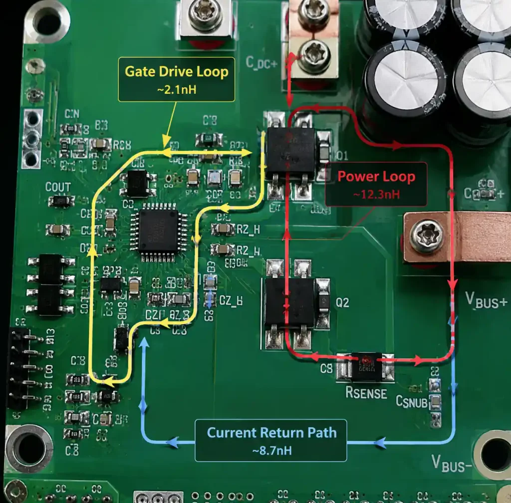
You must design power electronics PCB with parasitic minimization as the primary objective, treating every trace as an inductor at switching frequencies above 100kHz.
Gate Driver Placement Strategy
Minimize Gate Loop Inductance
The gate drive loop consists of the gate driver output, gate resistor, MOSFET gate terminal, source terminal, and return path to driver ground. Every millimeter of trace length adds approximately 1nH of inductance, and gate loop inductance above 5nH causes significant voltage overshoot and ringing.
Place gate driver IC within 10mm of the power MOSFET gate terminal. Route gate and source traces as a differential pair with maximum coupling to cancel mutual inductance. Reducing gate loop inductance from 15nH to 5nH decreases turn-on time from 35ns to 18ns and reduces gate ringing amplitude by 60%.
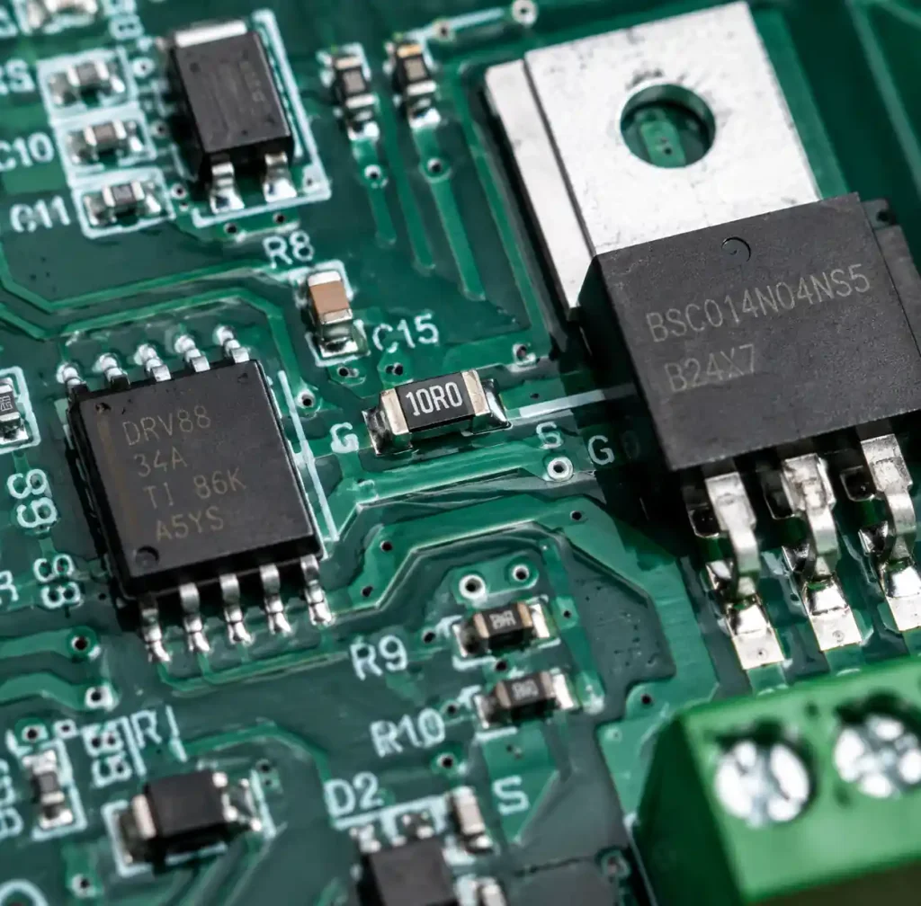
Use wide, short traces for gate connections (minimum 0.5mm width for currents up to 2A peak). Place gate resistor directly at the MOSFET gate pin, not at the driver output, to dampen parasitic oscillations at the device itself.
| Parameter | Target Value | Impact | Design Rule |
|---|---|---|---|
| Gate Loop Inductance | <5nH | Voltage overshoot, ringing | Driver within 10mm of gate |
| Gate Trace Width | ≥0.5mm | Current capacity, inductance | Wide, short routing |
| Gate Resistor Placement | At MOSFET pin | Damping effectiveness | Component at device terminal |
| Source Return Path | <3mm length | Common-mode noise | Dedicated Kelvin connection |
Kelvin Source Connection
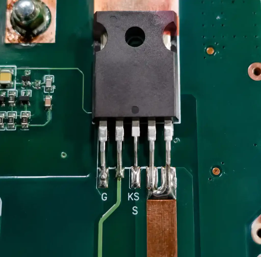
Kelvin source connection separates the high-current source path from the low-current gate drive return path. This eliminates common source inductance (CSI) that couples drain current di/dt noise directly into the gate drive signal.
Implement Kelvin source by routing gate driver ground directly to a dedicated source pad on the MOSFET package, separate from the power source connection. Modern SiC MOSFETs in TO-247-4 packages provide a dedicated Kelvin source pin. For TO-220 and D2PAK packages without Kelvin pin, route gate return trace to the source terminal location closest to the die bond wire inside the package.
Kelvin connection reduces turn-on switching loss by 15-25% and eliminates false turn-on risk during high di/dt transients. For a 1200V SiC MOSFET switching 20A with di/dt of 5A/ns, 5nH common source inductance generates 25V noise in the gate drive path—enough to cause unintended turn-on.
Switching Loop Minimization
Power Loop Layout
The switching loop carries high di/dt current during MOSFET transition and generates the strongest electromagnetic field in the converter. Minimize this loop area to reduce radiated EMI and voltage overshoot caused by loop inductance (V = L × di/dt).
The critical switching loop includes: DC bus capacitor → high-side MOSFET drain → switching node → low-side MOSFET source → ground plane → capacitor ground return. Place DC bus decoupling capacitors (typically 1-10μF ceramic) within 5mm of MOSFET drain and source terminals.
Reducing power loop area from 200mm² to 50mm² decreases switching node ringing by 40V and improves EMI performance by 12dB at 100MHz. Use multilayer PCB with power and ground planes on adjacent layers (50-100μm separation) to create distributed capacitance and minimize loop inductance.
| Loop Type | Target Area | Inductance Goal | Capacitor Placement |
|---|---|---|---|
| High-Side Switching Loop | <50mm² | <10nH | Within 5mm of drain/source |
| Low-Side Switching Loop | <50mm² | <10nH | Direct terminal connection |
| Gate Drive Loop | <100mm² | <5nH | Driver within 10mm |
| Snubber Loop | <20mm² | <5nH | Directly across device |
Half-Bridge Switching Node Layout
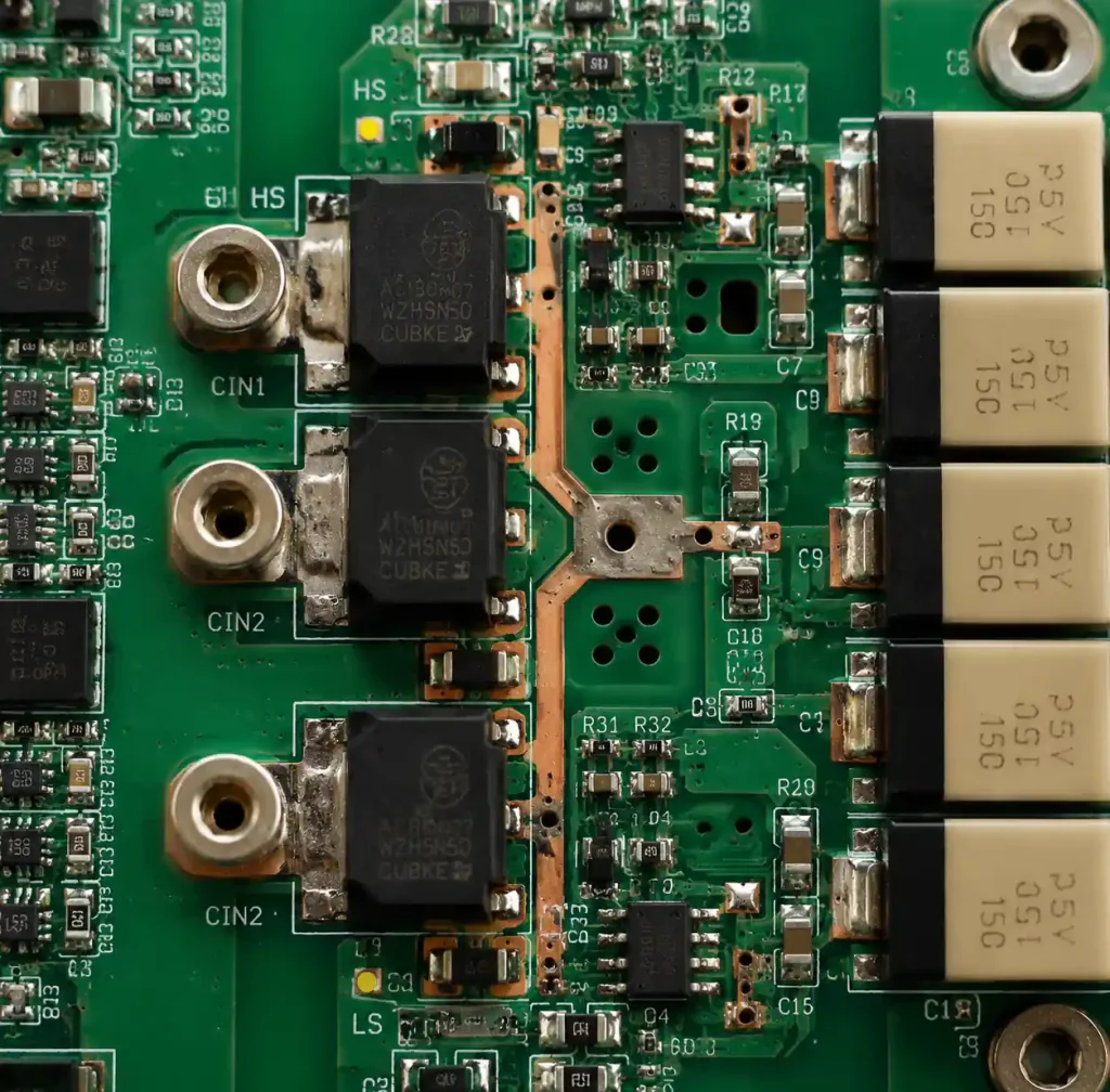
The switching node in half-bridge topology experiences voltage slew rates exceeding 50V/ns in GaN and SiC converters. Minimize switching node copper area and keep trace length under 3mm to reduce parasitic capacitance that increases switching loss through Qoss charging.
Route switching node as controlled impedance trace when connecting to remote loads beyond 10mm. Use ground plane cutouts beneath the switching node trace to prevent capacitive coupling. Place snubber RC network directly across drain-source terminals with trace length under 5mm.
Ground Plane Strategy
Star Grounding for Mixed-Signal Designs
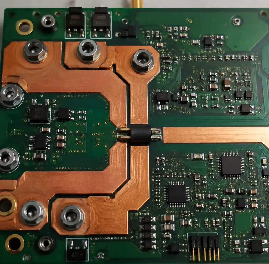
Power electronics PCB contains multiple ground domains: power ground (PGND), gate driver ground (DGND), and control logic ground (AGND). Improper connection creates ground loops where high di/dt power currents inject noise into sensitive control signals.
Implement star grounding where all ground domains connect at a single point near the power source. Route power ground as thick copper (2oz minimum) to carry high RMS current. Separate analog ground plane from power ground and connect at the star point through a 600Ω@100MHz ferrite bead. This reduces conducted noise coupling by 20-25dB in the 100kHz to 10MHz range.
Thermal Via Placement Strategy
Power MOSFETs and IGBTs dissipate significant heat during conduction and switching. Modern 100V MOSFETs in PQFN5×6 packages have thermal resistance of 1°C/W junction-to-case, requiring effective thermal path through PCB.
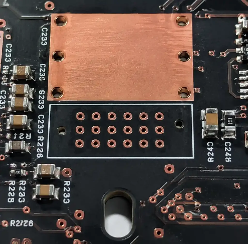
Place thermal via array directly beneath MOSFET thermal pad with via diameter 0.3-0.4mm and spacing 1.0-1.2mm center-to-center. Use minimum 16 vias for 5×6mm packages and 25+ vias for 8×8mm packages. Connect thermal vias to large copper area on bottom layer (minimum 500mm²). According to IPC-2152, 0.35mm diameter thermal vias with 1mm spacing reduce thermal resistance by 15-20°C/W.
| Device Package | Thermal Pad Size | Via Count | Via Diameter | Target θJA |
|---|---|---|---|---|
| PQFN 5×6mm | 3.5×4.5mm | 16-20 | 0.3mm | <40°C/W |
| PQFN 8×8mm | 6×6mm | 25-36 | 0.35mm | <30°C/W |
| TO-252 (DPAK) | 6×5mm | 20-25 | 0.35mm | <35°C/W |
| TO-263 (D2PAK) | 9×10mm | 36-49 | 0.4mm | <25°C/W |
Snubber Circuit Placement
RC Snubber Design and Layout
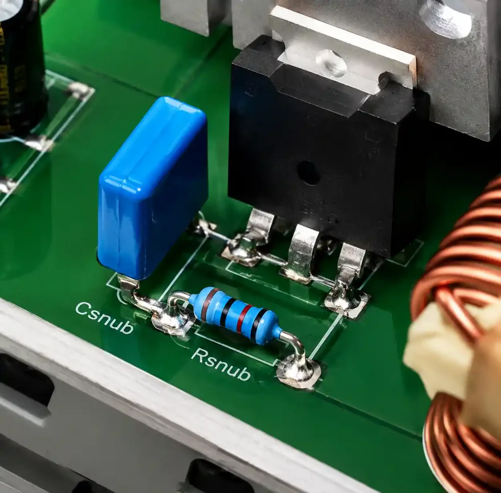
RC snubbers dampen voltage ringing caused by parasitic inductance and capacitance resonance during switching. Proper placement is critical—a well-designed snubber placed 20mm away provides minimal damping due to additional trace inductance.
Place snubber resistor and capacitor directly across MOSFET drain-source terminals with total trace length under 5mm. Use low-inductance film capacitors (0.1-1μF) rated for voltage 2× DC bus voltage. Select resistor value using R = √(L/C) where L is switching loop inductance. For a 400V half-bridge with 20nH loop inductance, optimal snubber uses 100nF capacitor and 15Ω resistor within 3mm of terminals.
Ferrite Bead Filtering
Gate driver power supply requires filtering to prevent switching noise feedback. Place 10μF bulk capacitor and 600Ω@100MHz ferrite bead at gate driver VDD pin with 1μF ceramic bypass capacitor at IC power pin. Route ferrite bead between bulk and bypass capacitors to create π-filter topology achieving 40dB noise rejection at 1MHz.
EMI Reduction Techniques
Common-Mode Choke and Filtering
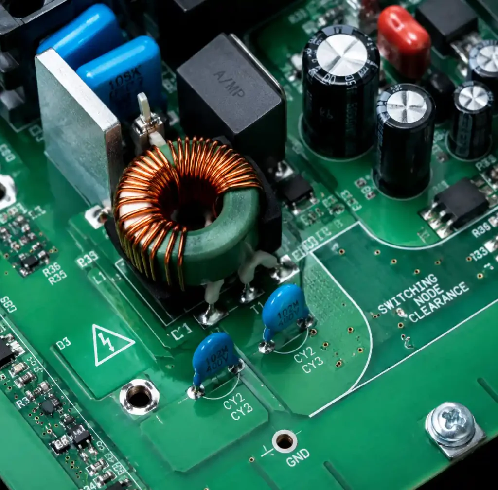
Switching power supplies generate differential-mode (DM) and common-mode (CM) noise. Common-mode noise couples through parasitic capacitance between switching node and ground plane, causing conducted EMI failures per CISPR 22 limits.
Place common-mode choke on DC input and AC output lines close to power stage. Use toroid core with high permeability (μi > 5000) and add Y-capacitors (1-10nF) from power lines to safety ground. Proper CM choke placement reduces conducted emissions by 15-20dB in the 150kHz to 30MHz range. Use ground plane under power traces but maintain 3-5mm clearance around switching node.
Shielding Strategy
SiC and GaN converters switching above 500kHz generate significant radiated EMI. Use multilayer stackup with ground planes on layers 2 and N-1 for electromagnetic shielding between power and control layers. Place sensitive analog traces on inner layers sandwiched between ground planes (stripline routing). For frequencies above 10MHz, use ground stitching vias at λ/10 spacing around board perimeter.
Power Trace Design Considerations
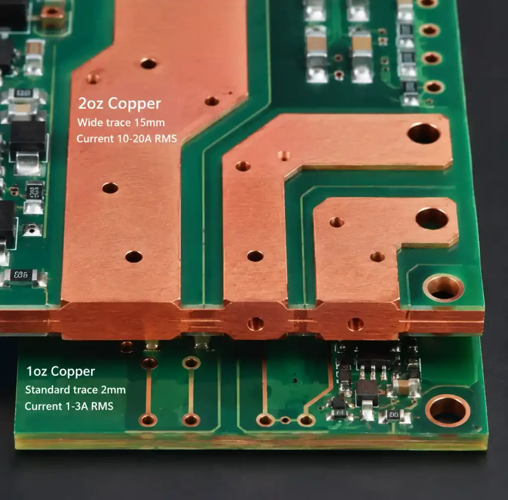
Power traces must carry high RMS current without excessive temperature rise. According to IPC-2152, 1oz (35μm) copper trace with 10mm width carries 5A with 10°C temperature rise. Use 2-4oz copper for power paths carrying more than 5A. For high-frequency applications, distribute current across multiple layers using via stitching to reduce AC resistance.
FAQ
What is the most critical layout rule for power electronics PCB?
Minimize switching loop inductance by placing DC bus capacitors within 5mm of MOSFET terminals. Every 1nH inductance generates 1V overshoot per 1A/ns current slew rate, so reducing loop area below 50mm² prevents destructive voltage spikes and improves EMI by 10-15dB.
How does Kelvin source connection improve switching performance?
Kelvin connection eliminates common source inductance that couples drain current di/dt noise into gate drive signal. This reduces turn-on switching loss by 15-25% and prevents false turn-on during high di/dt transitions.
What copper weight should I use for power traces?
Use 2oz (70μm) copper minimum for traces carrying more than 5A continuous current. A 10mm wide trace in 2oz copper carries 10A with 10°C temperature rise per IPC-2152.
Where should I place the gate resistor?
Place gate resistor directly at MOSFET gate pin, not at driver output, to dampen parasitic oscillations at device terminals. Typical values range from 2.2Ω to 10Ω depending on gate charge and desired switching speed.
How many thermal vias do I need under power MOSFETs?
Use minimum 16 vias (0.3mm diameter) for 5×6mm packages and 25+ vias for 8×8mm packages, with 1mm spacing. Connect vias to large copper area (>500mm²) on bottom layer to reduce thermal resistance by 15-20°C/W.
Conclusion
Effective power electronics PCB layout requires gate driver placement within 10mm of MOSFET gate, Kelvin source connection to eliminate common inductance, switching loop area below 50mm², and strategic ground plane separation. Thermal via arrays and snubber placement within 5mm of terminals complete the critical elements.
If you need power electronics PCB with controlled impedance, metal core substrates for thermal management, or multilayer boards up to 50 layers, Andwin Circuits delivers precision manufacturing with fast 7-day turnaround. Our power and energy PCB solutions meet automotive and industrial requirements with 100% electrical testing and IPC-A-600 Class 3 quality.
Contact us today for custom power electronics PCB manufacturing services with factory-direct pricing.