impedance control pcb

impedance control pcb
impedance control pcb
Base Material: TU-872 SLK SP/Arlon/Taconic/Isola/F4B/TP-2
Solder Mask Color: Green/ Blue/ Red/Yellow/Black/White
Silkscreen Color: Black/White
Surface Finished: HASL/HASL Lead Free/Immersion Gold/OSP
Package: Vacuum Package
Service: One-Stop Service
MOQ: 1 Piece
Description
1.What is the impedance control or a controlled impedance?
Impedance is the result of the interaction between the resistance and reactance in a circuit and expressed in Ohms. Impedance is an AC characteristic, which means it is related to frequency. A controlled impedance is important to maintain signal integrity, especially for high-frequency products

2. How to design a board with controlled impedance?
You should follow the below-mentioned controlled impedance routing tactics for designing a PCB:
2.1 Determine which signals require CI
Most of the time, electrical engineers specify which signal nets require a specific controlled impedance. However, if they do not, the designer should review the datasheets of the integrated circuits to determine which signals require controlled impedance. The datasheets usually provide detailed guidelines for each group of signals and their impedance values. The spacing rules and information on which layer to route specific signals may also appear in the datasheets or in the application notes. DDR traces, HDMI traces, Gigabit Ethernet traces, RF signals are some examples of controlled impedance traces.
2.2 Annotate the schematic with impedance requirements

2.3 Determine the trace parameters for controlled CI
A PCB trace is defined by its thickness, height, width, and dielectric constant (Er) of the PCB material on which the traces are etched.
While designing controlled impedance PCBs, it is essential to take care of these parameters. You can provide the manufacturer with the number of layers, the value of the impedance traces on specific layers (50Ω, 100Ω on layer 3), and materials for PCB designing.
The manufacturer gives you the stackup that mentions the trace widths on each layer, the number of layers, the thickness of each dielectric in the stackup, trace thickness, and PCB material. He also takes care of the controlled impedance requirements by calculating the feasible thickness, width, and height for the traces that need impedance control. Stick to the following relationships to know how impedance depends on dimensions:
- Impedance is inversely proportional to trace width and trace thickness
- Impedance is proportional to the laminate height and it is inversely proportional to the square root of laminate’s dielectric constant (Er).

3.When to Use Controlled Impedance
When a signal must have a particular impedance in order to function properly, controlled impedance should be used. In high frequency applications matching the impedance of PCB traces is important in maintaining data integrity and signal clarity. If the impedance of the PCB trace connecting two components does not match the components’ characteristic impedance, there may be increased switching times within the device or the circuit. There may also be random errors.

4.Why need impedance control in PCB design?
The traces in the PCBs are used to transfer maximum signal power from the source to the load. If the source’s impedance value does not match the impedance value of the load, some signals will be reflected back to the source. Then only part of the signals travels to the destination. As the demand for high-density and high-speed PCBs has increased dramatically, the PCB designs with controlled impedance have become very popular.
We may be no need to worry about the impedance control if the traces are short or low-frequency. But the reactance and the impedance are vital factors for high-frequency circuits. The higher the frequency, or the longer the traces, the more necessary it is to control the traces’ impedance.

5.Measuring controlled impedance
Impedance measurements are usually made with a time domain reflectometer (TDR). The TDR applies a fast voltage step to the coupon via a controlled impedance cable and probe. Any reflections in the pulse waveform are displayed on the TDR and indicate a change in impedance value (this is known as a discontinuity). The TDR is able to indicate the location and scale of discontinuity. Using appropriate software the TDR can be made to plot a graph of the impedance over the length of the test trace on the coupon. The resulting graphical representation of the trace characteristic impedance allows previously complex measurements to be performed in a production environment.

6.Applications of Controlled Impedance
Controlled Impedance should be considered for PCBs used in fast digital applications such as:
- Telecommunications
- Computing 100MHz and above
- High Quality Analog Video
- Signal Processing
- RF Communication

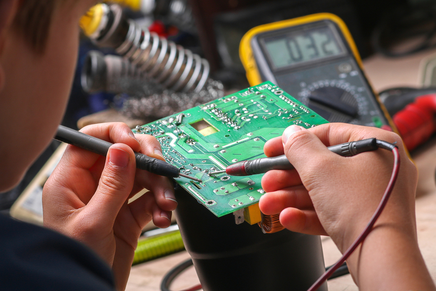
7.Testing the PCB
Most controlled impedance PCBs undergo 100% testing. However, it is not uncommon for the actual PCB traces to be inaccessible for testing. In addition, traces may be too short for accurate measurement and may well include branches and vias which would also make exact impedance measurements difficult. Adding extra pads and vias for test purposes would affect performance and occupy board space. PCB testing is therefore normally performed, not on the PCB itself, but on one or two test coupons integrated into the PCB panel. The coupon is of the same layer and trace construction as the main PCB and includes traces with precisely the same impedance as those on the PCB, so testing the coupon affords a high degree of confidence that the board impedances will be correct.
About Andwin Circuits
Andwin Circuits as a industry leading of PCB manufacturer since 2003.
Specializing in multilayer PCB, Rigid flex PCB, HDI PCB, controlled impedance PCB and Radio Frequency circuit, from quick turn prototype to mass products.