
IoT PCB Design: Power Management and Wireless Communication Best Practices
IoT devices operate in three power states. Active mode consumes 20-150 mA during sensing and transmission. Sleep mode draws 5-50 µA and covers 99% of operational time. Deep sleep mode uses less than 10 µA when all non-essential circuits shut down. Poor power management and RF layout mistakes cause 40% of IoT product failures in field deployments.
If you want to design IoT PCBs that achieve multi-year battery life and reliable wireless connectivity, then you will need to understand power distribution network optimization, low-quiescent-current regulator selection, RF trace impedance control, antenna placement rules, and mixed-signal layout techniques for WiFi, BLE, LoRa, and NB-IoT protocols.
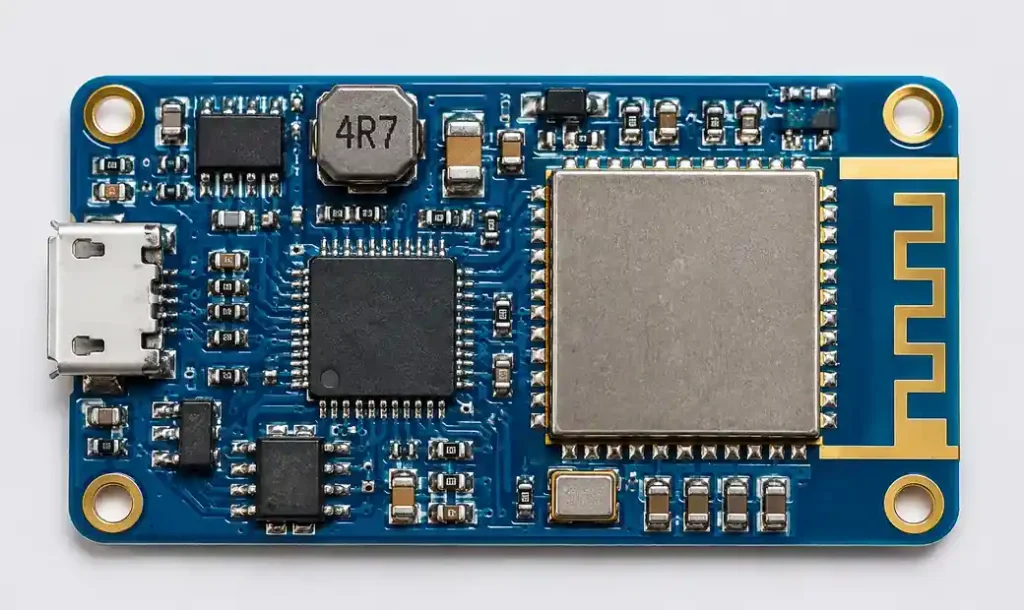
What is IoT PCB Design?
IoT PCB design integrates ultra-low-power microcontrollers, wireless transceivers, sensor interfaces, and power management circuits on compact boards measuring 15mm × 20mm to 50mm × 50mm. These designs must support coin cell or small lithium battery operation for 2-10 years while maintaining reliable wireless communication in challenging RF environments.
The core challenge is balancing three competing requirements: minimizing power consumption to extend battery life, maintaining signal integrity for wireless protocols operating at 433 MHz to 2.4 GHz, and fitting all components into space-constrained enclosures. You can use HDI PCB technology with laser-drilled microvias and 4-8 layers to achieve the routing density and RF performance required for modern IoT devices.
IoT applications span smart home devices, wearable health monitors, industrial sensors, asset trackers, and agricultural monitoring systems. Each application demands specific wireless protocols and power profiles based on data rate, range, and duty cycle requirements.
Power Management Architecture for IoT Devices
Power management determines IoT device battery life more than any other design factor. A poorly designed power distribution network wastes 30-50% of battery capacity through quiescent current, voltage conversion losses, and inadequate sleep mode implementation.
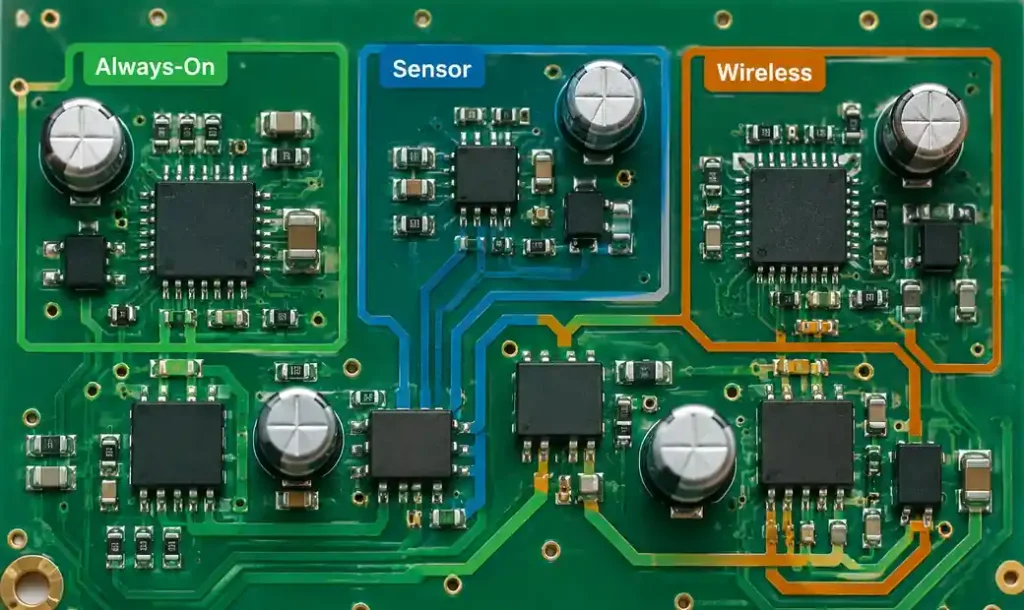
Low-Quiescent-Current Regulator Selection
Linear regulators for IoT applications must have quiescent current below 1 µA to avoid draining batteries during 99% sleep time. Standard LDOs with 50-100 µA quiescent current consume more power than the sleeping microcontroller, reducing battery life by 40-60%.
Use buck converters with power-save mode for input voltages above 3.6V. These converters achieve 85-92% efficiency at light loads by reducing switching frequency proportional to output current. Specify load-switch regulators with less than 50 nA leakage for sensor power domains that activate only during measurement cycles.
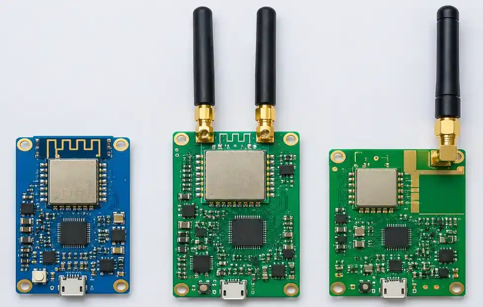
Power Domain Partitioning
Partition your IoT PCB into three power domains: always-on domain for RTC and wake logic (under 5 µA), sensor domain that activates for measurements (1-20 mA for 10-500 ms), and wireless domain for data transmission (20-150 mA for 5-50 ms). Each domain requires dedicated load switches controlled by GPIO pins to completely disconnect unused circuits.
Place decoupling capacitors within 2mm of IC power pins. Use 10 µF bulk capacitors for wireless transceiver power supply to handle 100+ mA transmission current spikes without voltage droop. Inadequate decoupling causes brownout resets during wireless transmission, appearing as intermittent connectivity failures.
Wireless Protocol Comparison for IoT Applications
| Protocol | Frequency | Range | Data Rate | Peak Current | Best For |
|—|—|—|—|—|
| BLE 5.0 | 2.4 GHz | 100m | 1 Mbps | 10-20 mA | Wearables, sensors |
| WiFi 6 | 2.4/5 GHz | 50-100m | 600 Mbps | 120-250 mA | Smart home, video |
| LoRa | 433/868/915 MHz | 2-15 km | 0.3-50 kbps | 30-45 mA | Asset tracking, agriculture |
| NB-IoT | Licensed LTE | 1-10 km | 250 kbps | 200-300 mA | Utility meters, infrastructure |
| Zigbee | 2.4 GHz | 10-100m | 250 kbps | 15-30 mA | Mesh networks, industrial |
RF Layout Best Practices for Wireless Protocols
RF layout mistakes cause 30-50% range reduction and intermittent connectivity in production IoT devices. Proper impedance control, ground plane design, and antenna placement are non-negotiable for reliable wireless performance.
Controlled Impedance for RF Traces
All RF traces connecting wireless transceivers to antennas must maintain 50-ohm characteristic impedance with ±10% tolerance. Use coplanar waveguide with ground (CPWG) geometry for surface layer RF traces: 0.3mm trace width with 0.2mm gap to ground pour on each side achieves 50 ohms on standard 1.6mm FR-4 with 4.3 dielectric constant.
Route RF traces on top or bottom layer only. Never route RF signals on inner layers where impedance control becomes impossible without expensive specialized stackups. Keep RF trace length under 30mm for 2.4 GHz signals and under 50mm for sub-GHz signals to minimize insertion loss.
Antenna Placement and Keep-Out Zones
Position antennas at board edges with no ground plane underneath for at least 5mm beyond the antenna element. PCB antennas require minimum 10mm × 10mm clear area for 2.4 GHz and 15mm × 20mm for 868/915 MHz LoRa designs. Placing ground plane under antenna reduces radiation efficiency by 60-80%, cutting range in half.
Space multiple antennas at least 15mm apart for WiFi and BLE coexistence designs. Closer spacing causes 5-10 dB isolation loss between antennas. Use separate ground planes with narrow connecting bridge if board size forces antennas closer than recommended minimum spacing.
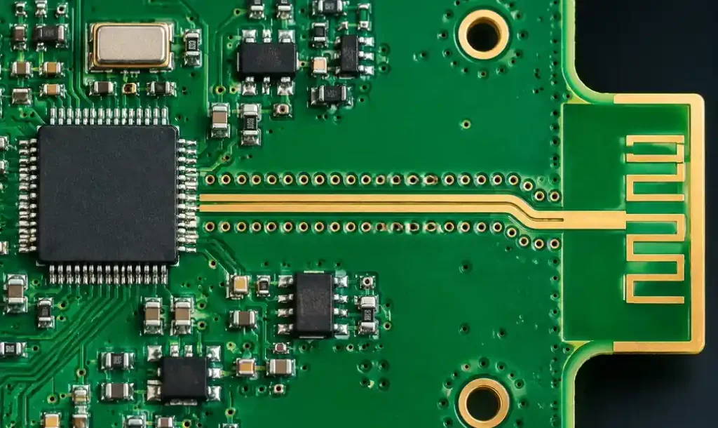
RF Ground Plane and Vias
Solid ground plane on layer 2 provides return path for RF signals and shields digital circuits from coupling into antenna. Place ground vias every 5mm along RF trace edges to create coplanar waveguide ground return. Missing or sparse via fencing causes 3-8 dB insertion loss and coupling to nearby circuits.
Never route high-speed digital signals under or near RF section. Keep crystal oscillators at least 10mm away from antenna and RF traces. Place RF section and antenna at opposite board end from switching power supplies to avoid conducted noise coupling.
Power Supply Design for Wireless Transmission
Wireless transmission creates 100-300 mA current spikes lasting 5-50 ms that must not cause voltage droop below minimum operating voltage. Inadequate power supply design causes failed transmissions and reduced range.
Bulk Capacitance for TX Current Spikes
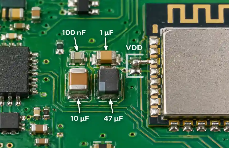
Place 10-22 µF ceramic capacitor within 5mm of wireless module VDD pin. This bulk capacitor supplies transmission current while slower DCDC converter responds to load step. Add 100 nF and 1 µF decoupling capacitors in parallel to handle high-frequency current components.
For WiFi designs requiring 200+ mA transmission current, use 47-100 µF tantalum or aluminum capacitor in parallel with ceramics. Ceramic capacitors alone cannot supply sustained high current without excessive ESR voltage drop.
DCDC Converter Transient Response
Buck converters for wireless applications need fast transient response with output voltage settling within 50 µs of load step. Specify converters with power-save mode that automatically increases switching frequency during transmission bursts. Poor transient response causes 0.2-0.5V voltage droop that triggers brownout reset.
Measure voltage at wireless module power pin during transmission using oscilloscope. Voltage droop exceeding 5% of nominal voltage indicates insufficient bulk capacitance or poor PCB power distribution network.
Battery Optimization Techniques
| Technique | Power Savings | Implementation | Applications |
|---|---|---|---|
| Sleep Mode | 95-99% | MCU deep sleep, peripheral power-off | All battery devices |
| Adaptive TX Power | 20-40% | Reduce transmit power based on RSSI | BLE, LoRa, Zigbee |
| Connection Intervals | 30-60% | Optimize BLE connection interval | Wearables, peripherals |
| Sensor Duty Cycle | 40-70% | Power sensors only during measurement | Environmental monitoring |
| Data Compression | 10-30% | Reduce TX time via compression | Long-range IoT |
Ultra-Low-Power Sleep Current
Achieving sub-10 µA sleep current requires eliminating all quiescent current sources. Disable unused MCU peripherals in firmware. Use power switches to completely disconnect sensor power supplies during sleep. Verify no pull-up or pull-down resistors create DC current paths to powered-off circuits.
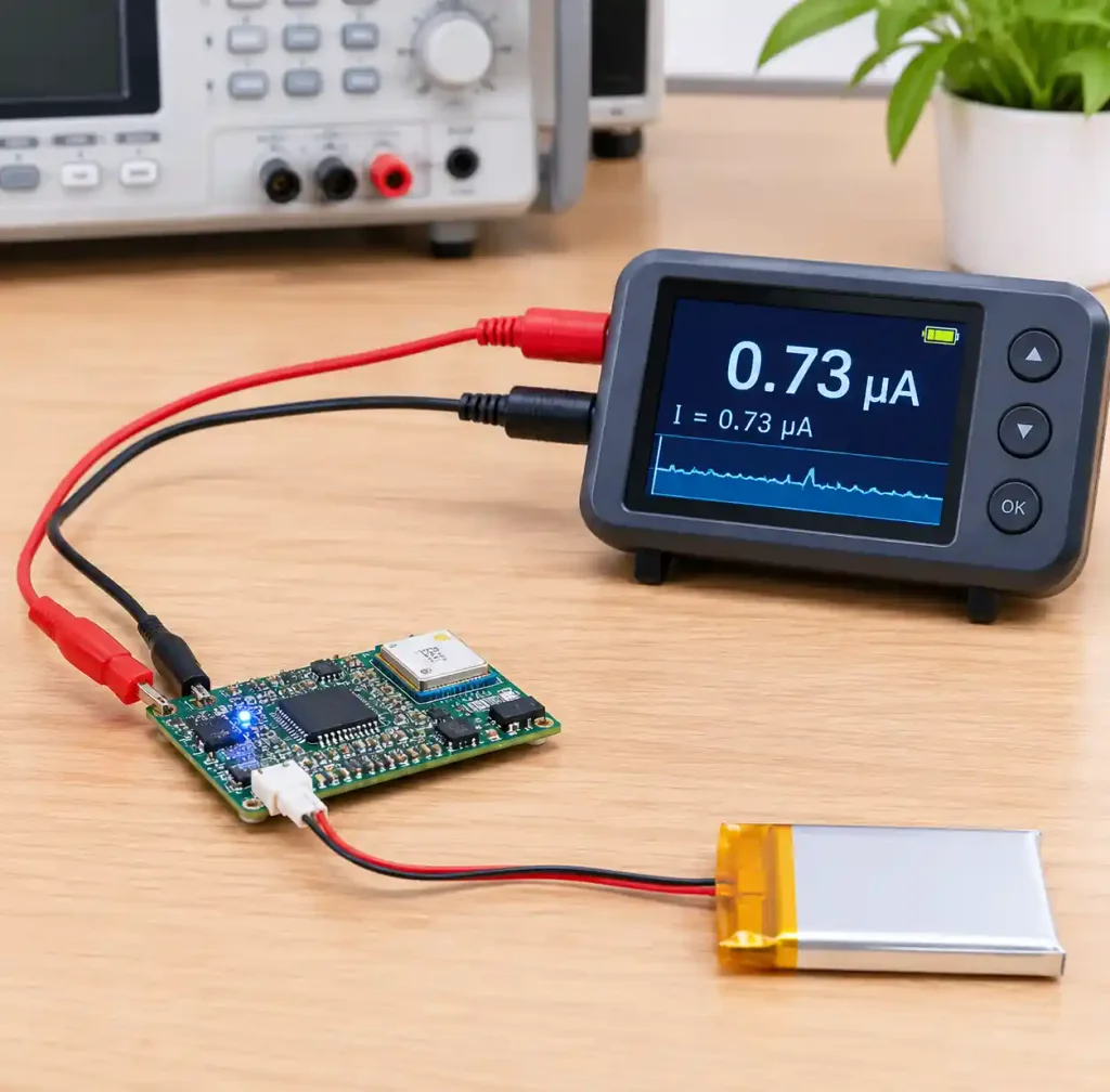
Measure actual sleep current using µCurrent or precision current meter. Many designs measure 50-200 µA sleep current due to forgotten pull-resistors, LED indicator current, or voltage regulator quiescent current. Each extra 10 µA reduces battery life by 15-25%.
Dynamic Voltage Scaling
Modern IoT MCUs support dynamic voltage and frequency scaling to reduce active current consumption. Running at 1.8V and 8 MHz instead of 3.3V and 48 MHz reduces active current by 60-70% for applications that do not need full processing speed.
Use lowest voltage and frequency that meets application timing requirements. Sensor data collection and basic processing typically requires only 4-8 MHz clock speed, not the 48-64 MHz maximum MCU speed.
BLE and WiFi Coexistence Design
IoT devices combining BLE and WiFi on single PCB face coexistence challenges because both protocols operate in 2.4 GHz band. Without proper design, WiFi transmission blocks BLE communication causing 20-40% packet loss.
Antenna Isolation and Filtering
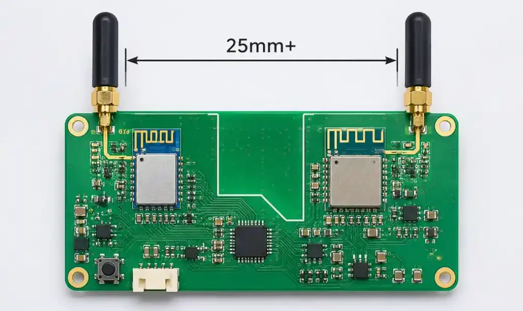
Use separate antennas for BLE and WiFi placed at opposite board corners with minimum 25mm spacing. This physical separation provides 15-20 dB isolation. Add 2.4 GHz bandpass filter on WiFi antenna feed to reduce harmonic emissions into BLE band.
Alternatively, use coexistence arbitration hardware that coordinates BLE and WiFi transmission timing to avoid simultaneous activity. Most modern wireless SoCs include three-wire coexistence interface for this purpose.
Time-Domain Multiplexing
Coordinate BLE advertising and WiFi transmission in firmware to avoid overlap. Schedule BLE connection events during WiFi idle periods. Use WiFi power-save mode (PS-Poll or U-APSD) to create regular idle windows for BLE communication.
This software coordination reduces coexistence packet loss from 30-40% to under 5% without additional hardware cost or board space.
LoRa and NB-IoT Design Considerations
Sub-GHz wireless protocols like LoRa (433/868/915 MHz) and NB-IoT require different PCB design approaches than 2.4 GHz protocols due to longer wavelengths and higher transmission power.
Sub-GHz Antenna Design
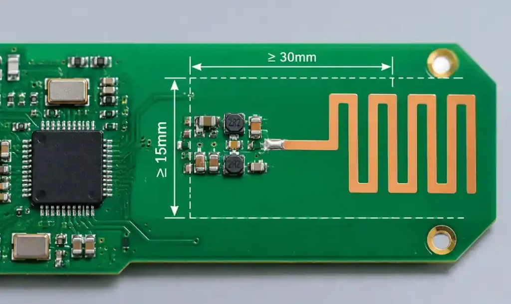
LoRa antennas require 30-80mm PCB length depending on frequency. Use meandered monopole or inverted-F antenna topology. Provide minimum 15mm × 30mm ground-plane-free area around antenna element. Sub-GHz antenna performance degrades less from nearby objects than 2.4 GHz antennas, allowing more placement flexibility.
Match antenna to 50-ohm transceiver output using pi or T-network. Tune matching network with network analyzer to achieve VSWR under 2:1 across operating band. Unmatched antenna reduces range by 30-50% and increases battery drain due to reflected power.
High-Power Transmission Considerations
LoRa and NB-IoT transmission power reaches +14 to +30 dBm (25-1000 mW) compared to 0-10 dBm for BLE. This high power creates 200-300 mA current spikes requiring 47-100 µF bulk capacitance and proper PCB power distribution.
Use 2oz or 3oz copper weight for power traces connecting battery to wireless module. Standard 1oz copper creates excessive voltage drop during high-current transmission pulses. Calculate trace width to limit voltage drop to under 50mV at maximum transmission current.
Mixed-Signal Layout for IoT Applications
IoT PCBs combine ultra-low-power analog sensors, high-speed digital MCU, and high-power RF circuits on compact boards. Proper partitioning and grounding prevent digital noise from corrupting sensor readings and RF performance.
Ground Plane Strategy
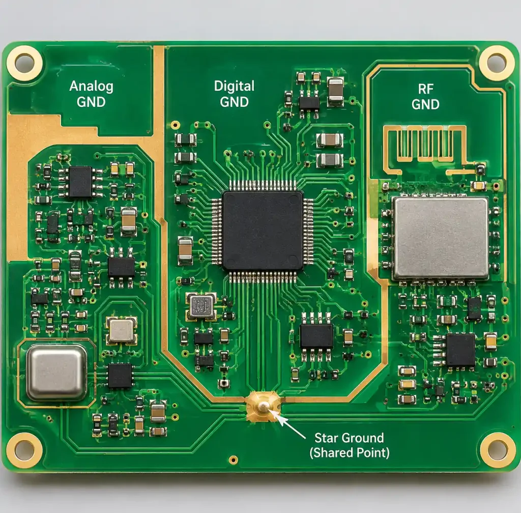
Use star ground topology with single-point connection between analog, digital, and RF ground sections. Connect ground sections under MCU analog power pins using 0.1-0.2mm width trace to minimize digital noise coupling. Never create multiple ground plane connections that form ground loops.
For 4-6 layer PCBs, dedicate layer 2 as solid ground plane and layer 3 as power plane. This provides low-inductance return path and minimizes EMI. Route sensitive analog signals on top layer with ground plane directly below on layer 2.
Sensor Interface Best Practices
Place analog sensors and their signal conditioning circuits in dedicated board section separated from MCU and wireless circuits by at least 10mm. Use ground plane split or narrow ground bridge to define analog section.
Route ADC input traces as differential pairs with guard traces connected to analog ground. Keep ADC trace length under 20mm to minimize noise pickup. Use RC filter on ADC inputs to eliminate high-frequency digital switching noise above ADC sampling bandwidth.
Frequently Asked Questions
What is the most important factor in IoT PCB power management?
Quiescent current of voltage regulators determines battery life more than any other factor. Regulators with 50-100 µA quiescent current drain batteries faster than sleeping MCUs. Specify regulators with under 1 µA quiescent current and use load switches to completely power off unused circuits.
How do I choose between WiFi, BLE, LoRa, and NB-IoT for my IoT device?
Choose based on data rate, range, and power requirements. BLE offers lowest power for short-range sensor data. WiFi provides high data rate for video and frequent updates. LoRa achieves 2-15 km range for infrequent sensor readings. NB-IoT uses cellular infrastructure for wide-area coverage without gateway requirements.
What causes poor WiFi or BLE range in IoT devices?
Ground plane under antenna is the most common cause, reducing range by 50-70%. Other issues include incorrect impedance control on RF traces, missing ground via fencing, inadequate antenna keep-out area, and insufficient bulk capacitance causing voltage droop during transmission.
How can I achieve 5-10 year battery life in IoT devices?
Reduce sleep current below 5 µA through proper regulator selection and power domain partitioning. Minimize transmission duty cycle by using adaptive intervals and data compression. Implement dynamic voltage scaling to reduce active current. Verify actual sleep current measurement matches design targets.
What PCB layer count do I need for IoT devices with wireless?
Four-layer PCB provides solid ground and power planes necessary for RF performance and adequate routing density for most IoT designs. Six-layer PCB offers better EMI performance and routing flexibility for complex designs with multiple wireless protocols and dense sensor arrays.
How do I prevent digital noise from affecting RF performance?
Use star ground topology with single-point connection between digital and RF grounds. Place RF section at board edge with antenna at corner. Keep crystal oscillators and switching power supplies away from RF section. Use ground via fencing along RF trace edges for shielding.
Conclusion
IoT PCB design success depends on three critical factors: ultra-low quiescent current power management to achieve multi-year battery life, controlled-impedance RF layout with proper antenna placement for reliable wireless connectivity, and mixed-signal partitioning to prevent digital noise from corrupting sensor and RF performance. Choosing appropriate wireless protocols based on range, data rate, and power requirements ensures optimal battery life and connectivity.
If you need high-quality IoT PCB manufacturing with advanced HDI technology for your wireless device projects, Andwin Circuits offers 4-50 layer capability with controlled impedance, RF design expertise, and fast delivery in 7 days for prototypes. Our ISO 9001 and IATF 16949 certified facility has delivered IoT PCBs for smart home, wearable, industrial sensing, and asset tracking applications worldwide with 100% quality guarantee.
Contact us today for custom IoT PCB manufacturing, RF layout review, and competitive factory-direct pricing for your next wireless product development.