
PCB Fiducial Marks: Types, Placement, and Vision System Requirements
Pick-and-place machines placing 30,000 components per hour achieve 25-micron accuracy only when vision systems lock onto precise reference points. PCB fiducial marks are exposed copper targets that enable automated optical inspection (AOI) and SMT equipment to align boards within tolerances that manual assembly cannot achieve. When fiducials fail, a misplaced 0.4 mm pitch BGA creates bridging defects costing $15-50 per board to rework.
What Are PCB Fiducial Marks?
PCB fiducial marks are solid copper reference features, typically circular, that remain exposed without solder mask coverage. They function as optical anchors for machine vision systems during SMT assembly, solder paste printing, and automated optical inspection.
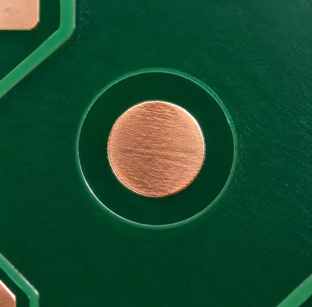
Vision cameras capture fiducial positions and calculate the board’s actual position relative to programmed coordinates. According to IPC-7351 standards, fiducials must provide sufficient contrast for optical recognition. The standard implementation uses a bare copper pad surrounded by solder mask clearance at least 2× the pad diameter, creating the dark-light boundary that vision algorithms detect.
Global vs Local Fiducials: When to Use Each
PCB designs require two fiducial categories based on assembly accuracy requirements. Global fiducials establish board-level alignment, while local fiducials refine positioning for critical components.
Global Fiducials
Global fiducials align the entire PCB relative to assembly equipment. You need minimum three global fiducials per board to provide rotational correction. Arrange them in a non-collinear pattern forming a wide triangle that maximizes distance between marks.
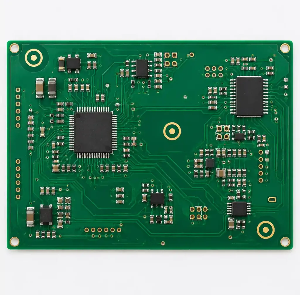
For rectangular PCBs, place global fiducials diagonally opposite corners. On a 100 mm × 150 mm board, fiducials separated by the full diagonal distance (180 mm) deliver 3× better rotational accuracy than marks only 60 mm apart.
Local Fiducials
Local fiducials sit near fine-pitch components where global board alignment alone cannot guarantee placement accuracy. Add local fiducials for components meeting these criteria:
| Component Type | Local Fiducial Trigger | Typical Pitch |
|---|---|---|
| Fine-pitch BGA | Pitch ≤ 0.5 mm | 0.4 mm, 0.5 mm |
| QFP/QFN packages | Lead pitch ≤ 0.4 mm | 0.3 mm, 0.4 mm |
| Micro-BGA | Any micro-BGA | 0.3 mm, 0.35 mm |
| High-value ICs | Unit cost > $50 | Varies |
Place two local fiducials diagonally across the component footprint, maintaining 50-100 mm separation. This creates a dedicated coordinate system for that component, reducing placement error from ±50 microns (global only) to ±25 microns.
Fiducial Size and Clearance Requirements
Vision system recognition depends on fiducial geometry meeting optical resolution limits and providing adequate contrast boundaries.
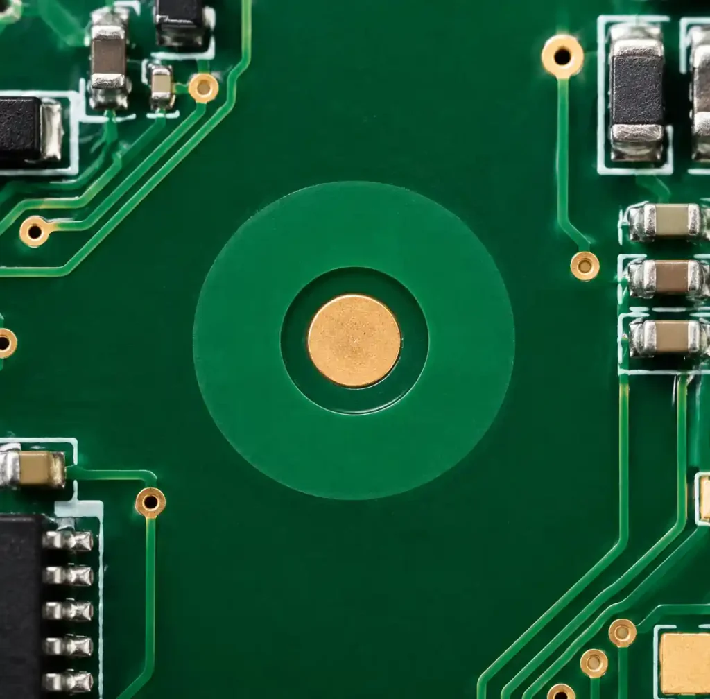
The most reliable fiducial size is 1.0 mm diameter copper pad with 2.0 mm solder mask opening. This 1 mm pad / 2 mm clearance ratio works across nearly all SMT equipment built after 2015.
| Fiducial Parameter | Minimum | Recommended | Maximum |
|---|---|---|---|
| Copper Pad Diameter | 0.75 mm | 1.0 mm | 3.0 mm |
| Solder Mask Opening | 1.5 mm | 2.0 mm | 5.0 mm |
| Keepout Zone (radius) | 1.5 mm | 3.0 mm | — |
| Edge Clearance | 3.0 mm | 5.0 mm | — |
The keepout zone around each fiducial must remain clear of traces, vias, silkscreen, and other copper features. Vision algorithms threshold image contrast, and nearby copper reduces edge definition.
Position global fiducials 5 mm minimum from board edges. Assembly tooling fixtures and panel clamps occupy edge zones. For panelized designs, place fiducials in the panel border area, not on individual boards.
Placement Guidelines for Maximum Recognition Accuracy
Fiducial placement directly affects vision system performance. Poor placement creates false detections, recognition failures, or degraded accuracy.
The most effective global fiducial pattern places three marks forming a large obtuse triangle. On rectangular boards, position one fiducial near each end of the board’s long axis, with the third mark offset from the centerline.
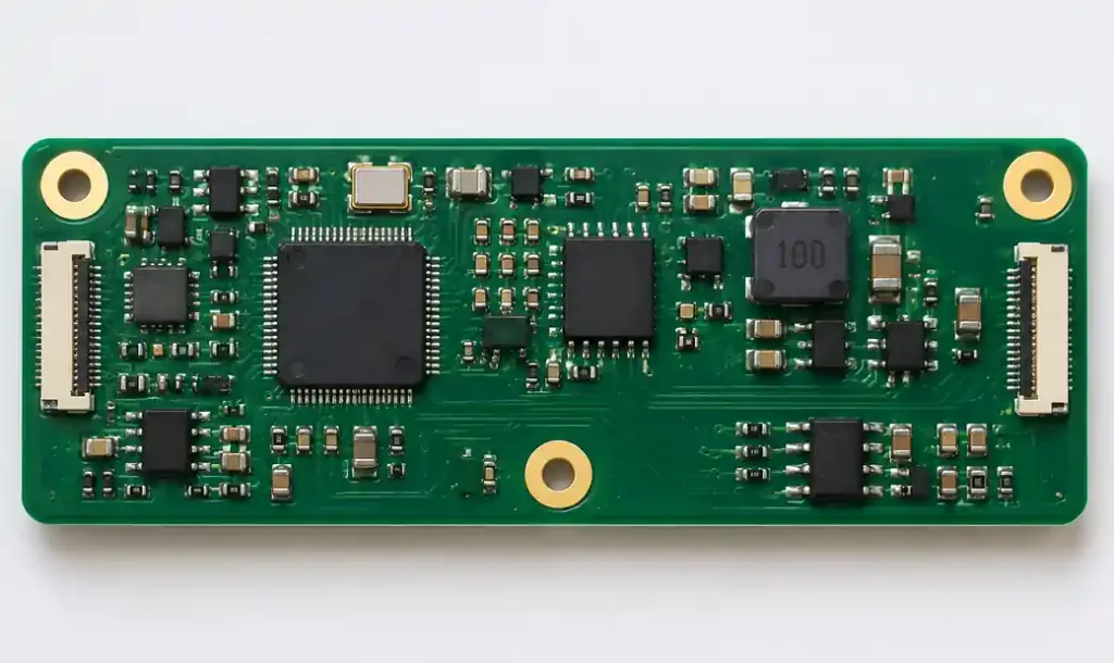
This asymmetric arrangement eliminates 180-degree rotational ambiguity. Symmetric fiducial placement prevents vision software from distinguishing between correct orientation and 180-degree inversion.
For double-sided PCB assembly, both sides require independent fiducial sets. The bottom-side camera must locate bottom-side fiducials—top-side marks provide no reference after board flip.
Panelized production needs both panel-level and board-level fiducials. Panel fiducials align the entire panel for paste printing; board fiducials align individual boards during component placement after depanelization. Place panel fiducials in tooling rails or border waste areas, maintaining the same 5 mm edge clearance.
Vision System Recognition Requirements
Modern SMT equipment uses machine vision to locate fiducials with sub-pixel accuracy, but recognition reliability depends on meeting specific requirements.
Bare copper fiducials provide maximum contrast against dark FR4 or solder mask backgrounds. Surface finishes affect recognition—ENIG (Electroless Nickel Immersion Gold) produces the best optical contrast due to its mirror-like gold surface.
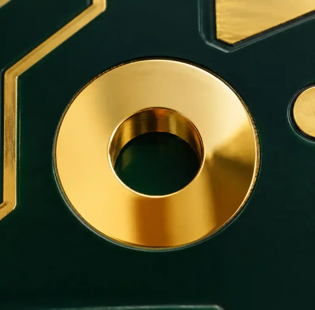
HASL (Hot Air Solder Leveling) creates less reliable fiducials because the solder coating produces non-uniform surface topology. OSP (Organic Solderability Preservative) works adequately but degrades after extended exposure to air or handling.
Vision systems use ring lights or coaxial illumination to image fiducials. Image processing algorithms locate fiducials through edge detection, identifying the circular boundary and calculating the centroid. Sub-pixel interpolation achieves 1-5 micron position accuracy.
Recognition fails when solder mask encroaches onto the copper pad, silkscreen overlaps the opening, copper oxidation darkens the surface, or board warpage moves the fiducial out of camera focal depth.
SMT Assembly Accuracy and Fiducial Impact
Component placement accuracy depends on fiducial-derived alignment corrections. Without fiducials, machines place components relative to panel edges—typically ±0.2 mm accuracy. Fiducial-based alignment improves this to ±0.025 mm.
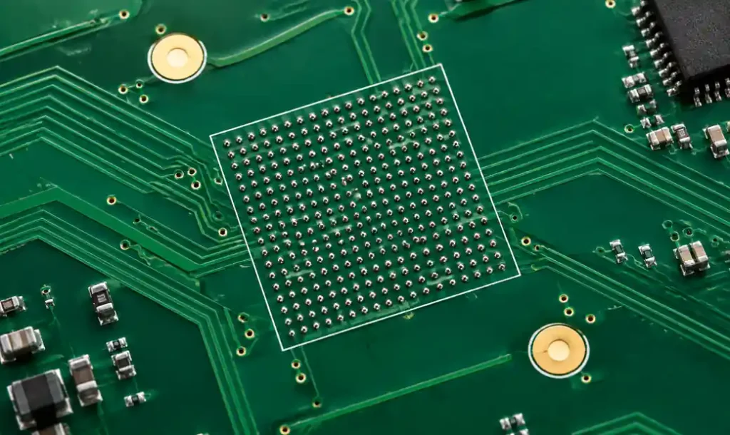
Total placement error combines multiple sources: board position error, machine repeatability, component dimensional tolerance, and thermal expansion during reflow. Fiducials eliminate board position error but cannot compensate for other factors.
| Error Source | Without Fiducials | With Global Fiducials | With Local Fiducials |
|---|---|---|---|
| Board positioning | ±200 μm | ±25 μm | ±25 μm |
| Machine repeatability | ±50 μm | ±50 μm | ±50 μm |
| Component tolerance | ±75 μm | ±75 μm | ±75 μm |
| Thermal expansion | ±30 μm | ±30 μm | ±10 μm |
| Total (RSS) | ±227 μm | ±104 μm | ±96 μm |
Components with 0.3-0.5 mm pitch require local fiducials to achieve acceptable yield. A 0.4 mm pitch BGA with 0.25 mm pad diameter tolerates only ±75 micron total placement error before solder bridging risk exceeds 1%.
For HDI PCB designs with multiple fine-pitch components, budget one local fiducial pair per component exceeding $20 unit cost or requiring ≤0.4 mm pitch.
Automated Optical Inspection (AOI) Applications
AOI equipment uses the same fiducials as placement machines to align inspection cameras with board features. After reflow, AOI systems image solder joints and compare them against golden board templates.
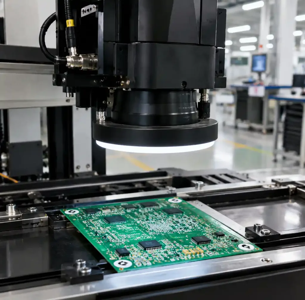
Fiducial-based alignment ensures the AOI camera looks at the correct location on every board. Without fiducials, board-to-board position variation creates false defect calls—the camera images offset from the actual component location.
AOI systems typically require only global fiducials because inspection occurs after placement when components themselves provide additional reference points. For double-sided assemblies, bottom-side AOI cannot use top-side fiducials, requiring independent bottom-side marks.
Common Fiducial Design Mistakes
Even experienced designers make fiducial errors that reduce assembly yield. These mistakes appear repeatedly across quick-turn PCB assembly projects.
Insufficient Solder Mask Clearance: Specifying 1 mm copper pad with 1.2 mm solder mask opening creates only 0.1 mm clearance ring—too narrow for reliable edge detection. Manufacturing tolerance on solder mask registration is ±0.075 mm, meaning the solder mask can partially cover the pad. Use 2× clearance ratio minimum: 1 mm pad needs ≥2 mm opening.
Collinear Fiducial Arrangement: Placing three fiducials in a straight line prevents rotational error detection. Vision systems calculate rotation from the angle between fiducials—collinear marks provide no rotational information. Maintain non-collinear geometry with the third fiducial offset at least 5 mm perpendicular to the line connecting the first two marks.
Silkscreen Over Fiducials: Component reference designators or company logos printed over fiducial keepout zones interfere with vision recognition. Silkscreen ink creates false edges that confuse edge-detection algorithms. Maintain 3 mm silkscreen clearance from fiducial centers.
Using Plated Holes: Drilled holes with copper plating are not valid fiducials. Vision systems detect circular solid features, not ring-shaped outlines. Holes also collect solder paste during printing, creating reflective solder balls that disrupt recognition. Only solid copper pads work as fiducials.
Design Checklist for Fiducial Success
Before sending Gerber files to your PCB manufacturer, verify your design meets these requirements:
Global Fiducials: Minimum three marks per board side; Non-collinear arrangement with maximum separation; 1.0 mm copper pad diameter (bare copper); 2.0 mm solder mask opening; 3.0 mm keepout radius; 5.0 mm minimum edge clearance.
Local Fiducials: Two marks per component with pitch ≤0.5 mm or cost ≥$50; Diagonal placement across component footprint; 50-100 mm mark separation; Same size specifications as global fiducials.
Documentation: Fiducial locations marked in assembly drawing; Fiducial coordinates in Centroid/XY file; Surface finish specified (ENIG recommended); Top-side vs bottom-side marks indicated.
FAQ
Can I use the same fiducials for both paste printing and component placement?
Yes. Solder paste printers and pick-and-place machines share the same fiducial marks. The printer uses them first to align the stencil, then the placement machine uses the same marks for component positioning.
What happens if my PCB has no space for standard 1 mm fiducials?
Reduce fiducial size to 0.75 mm copper pad with 1.5 mm solder mask opening, but verify your assembly house can recognize smaller marks before production. Alternatively, place fiducials in panel tooling rails rather than on individual boards.
Do I need fiducials on both sides of a double-sided PCB?
Yes, when both sides require component assembly. After placing top-side components and flipping the board, bottom-side cameras need visible fiducials for alignment. Use three independent fiducials per side, totaling six marks minimum.
How many fiducials does a panelized design need?
Panel designs require both panel-level fiducials (for paste printing) and board-level fiducials (for component placement). Place minimum three panel fiducials in border areas, plus three fiducials on each individual board.
What surface finish provides the best fiducial recognition?
ENIG (Electroless Nickel Immersion Gold) produces optimal fiducials due to its flat, highly reflective gold surface that creates maximum contrast. HASL works but has less reliability. OSP is acceptable but degrades with handling.
Conclusion
Proper fiducial design directly determines SMT assembly yield and placement accuracy. Vision systems require clearly defined reference marks to achieve the 25-50 micron precision that fine-pitch components demand. A 1 mm diameter bare copper pad surrounded by 2 mm solder mask clearance, positioned with adequate edge margins and keepout spacing, provides reliable recognition across all modern placement equipment. Global fiducials align the entire board; local fiducials refine positioning for critical components.
Andwin Circuits provides DFM review for fiducial placement and assembly optimization. Contact our engineering team to verify your design meets vision system requirements before production.