
PCB for Harsh Chemical Environments: Material and Coating Selection
When electronics operate in chemical processing plants, industrial manufacturing facilities, or oil and gas installations, standard PCB materials fail rapidly. Chemical exposure degrades substrates, dissolves coatings, and corrodes copper traces—leading to catastrophic failures that halt production lines. Selecting the right materials and protective coatings isn’t optional; it’s the difference between reliable operation and costly downtime.
This guide examines substrate materials and coating technologies that withstand aggressive chemical environments, drawing from field deployment data and accelerated testing protocols used by manufacturers serving industrial markets.
Understanding Chemical Attack Mechanisms on PCBs
Chemical damage to PCBs follows predictable failure modes. Organic solvents penetrate epoxy matrices, causing delamination between copper and substrate. Acids etch exposed copper traces, creating open circuits. Bases attack glass fibers in FR-4 laminates, weakening mechanical integrity. Oxidizing agents degrade polymer chains in both substrates and conformal coatings.
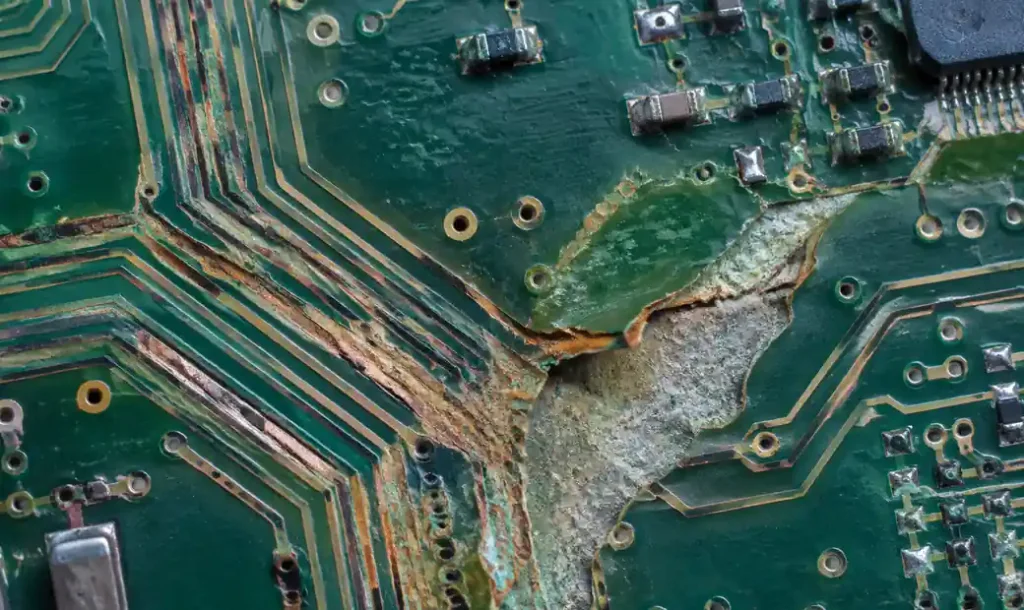
The severity depends on three factors: chemical concentration, exposure temperature, and contact duration. A PCB surviving brief solvent splashes at room temperature may fail within hours when continuously immersed at 60°C. Standard FR-4 boards show measurable degradation after 500 hours in 10% sulfuric acid at 40°C, while specialized polyimide substrates maintain integrity beyond 2,000 hours under identical conditions.
Substrate Material Selection for Chemical Resistance
FR-4: Baseline Performance and Limitations
FR-4 epoxy-glass composite dominates general electronics, but its chemical resistance has clear boundaries. The epoxy resin absorbs moisture and swells when exposed to polar solvents like acetone, methanol, or isopropanol. Continuous exposure to concentrations above 50% causes measurable dimension changes within 100 hours.
Testing data shows FR-4 maintains electrical properties when exposed to dilute acids (pH > 3) and weak bases (pH < 11) at temperatures below 40°C. Beyond these parameters, glass fiber exposure accelerates as the epoxy matrix degrades. High-Tg FR-4 variants (Tg 170-180°C) offer improved thermal stability but provide minimal improvement in chemical resistance.
| Chemical Class | FR-4 Compatibility | Typical Failure Mode | Safe Exposure Limit |
|---|---|---|---|
| Aliphatic Hydrocarbons | Good | None observed | Continuous |
| Aromatic Solvents | Poor | Matrix swelling | < 100 hours |
| Concentrated Acids | Poor | Copper etching | < 50 hours |
| Strong Bases | Poor | Glass fiber attack | < 24 hours |
| Chlorinated Solvents | Moderate | Epoxy softening | < 200 hours |
Polyimide: Premium Chemical Resistance
Polyimide substrates deliver superior chemical resistance through their dense, cross-linked molecular structure. The material resists swelling in most organic solvents and maintains dimensional stability when exposed to acids and bases that rapidly destroy FR-4.
Field deployments in chemical processing environments show polyimide PCBs operating reliably for 3-5 years with minimal degradation, compared to 6-12 months for FR-4 in identical conditions. The material’s glass transition temperature exceeds 250°C, allowing operation in high-temperature chemical processes where FR-4 would delaminate.
Polyimide’s primary limitation is cost—typically 3-5 times higher than FR-4 per square meter. However, extended service life and reduced replacement frequency offset the initial premium in harsh environment applications. The material also requires modified drilling and routing parameters, as its toughness causes accelerated tool wear compared to FR-4.
PTFE-Based Laminates: Extreme Chemical Immunity
PTFE (polytetrafluoroethylene) composites offer the highest chemical resistance among PCB substrates. The fluoropolymer matrix remains inert to virtually all industrial chemicals except molten alkali metals and fluorine gas at elevated temperatures. PTFE laminates maintain electrical and mechanical properties after prolonged exposure to concentrated acids, strong oxidizers, and chlorinated solvents that destroy both FR-4 and polyimide.
Applications requiring PTFE substrates include circuit boards deployed in electrochemical cells, chlorine production facilities, and semiconductor wet processing equipment. The material’s extremely low moisture absorption (< 0.01%) prevents electrical parameter drift in humid chemical environments.
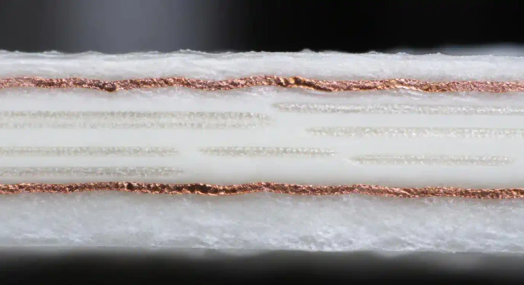
PTFE’s cost exceeds polyimide by 2-3 times, and its mechanical properties create manufacturing challenges. The material’s low surface energy requires specialized cleaning and surface treatment before coating application. PTFE also exhibits significant thermal expansion—demanding careful via design to prevent barrel cracking during temperature cycling.
Conformal Coating Technologies for Chemical Protection
Acrylic Coatings: Entry-Level Protection
Acrylic conformal coatings provide basic moisture barrier properties and protection against mild chemical splash. The coatings apply easily via spray, brush, or dip methods and remain reworkable with common solvents—simplifying field repairs.
Chemical resistance is limited. Aromatic solvents, ketones, and esters rapidly soften acrylic films, creating pathways for contamination to reach component surfaces. Testing shows film degradation begins within 24 hours when exposed to toluene, methyl ethyl ketone, or ethyl acetate. Acrylic coatings suit applications with occasional mild chemical exposure but fail in continuous immersion or high-concentration environments.
Silicone Coatings: Temperature and Flexibility
Silicone conformal coatings excel in high-temperature applications, maintaining flexibility from -55°C to 200°C. The material’s chemical resistance surpasses acrylics, particularly against polar solvents and dilute acids. Silicone films remain intact after 1,000 hours of exposure to 10% hydrochloric acid or 10% sodium hydroxide at 40°C.
The coating’s high flexibility accommodates thermal expansion mismatch between components and PCB substrates, reducing stress-induced cracking. This property proves essential when protecting PTFE-based boards, which expand significantly during temperature cycling.
Silicone’s primary disadvantage is its low abrasion resistance. Mechanical contact from mating connectors or maintenance activities easily damages the film. The material also exhibits high moisture vapor transmission compared to other coating types—limiting effectiveness in combined chemical and humidity environments.
Urethane Coatings: Robust Chemical Barriers
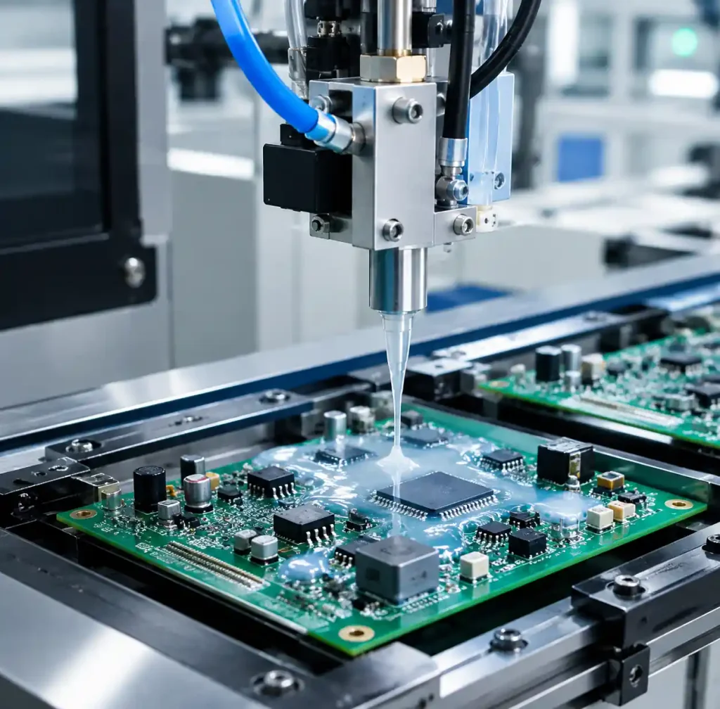
Polyurethane conformal coatings deliver excellent resistance to oils, fuels, and aliphatic solvents. The dense, cross-linked polymer network creates an effective barrier against moisture and ionic contaminants. Urethane films withstand continuous immersion in hydraulic fluids, diesel fuel, and mineral oils without measurable degradation.
Chemical resistance testing demonstrates urethane coatings maintain dielectric strength after 2,000 hours exposure to 3% sodium chloride solution at 50°C. The material resists fungal growth and provides superior abrasion resistance compared to silicone or acrylic alternatives.
Urethane coatings require careful application technique. The materials are moisture-sensitive before curing and demand low-humidity environments (< 50% RH) during deposition. Once cured, removal for rework requires aggressive solvents or mechanical grinding—making repairs time-intensive.
Parylene: Maximum Chemical Protection
Parylene coatings, deposited via chemical vapor deposition, provide the highest chemical resistance and most uniform coverage of any conformal coating technology. The process creates a pinhole-free polymer film that penetrates under components and into tight spaces inaccessible to liquid coatings.
Parylene C and Parylene N variants resist aggressive chemicals including strong acids, concentrated bases, and most organic solvents. Testing shows no measurable degradation after 5,000 hours in 30% sulfuric acid, 30% sodium hydroxide, or pure trichloroethylene. The coating’s extremely low moisture permeability (< 0.01 g/100 in²/day) prevents corrosion in combined chemical and humidity environments.
| Coating Type | Chemical Resistance | Moisture Protection | Reworkability | Relative Cost |
|---|---|---|---|---|
| Acrylic | Fair | Good | Excellent | 1.0x |
| Silicone | Good | Fair | Good | 1.5x |
| Urethane | Very Good | Excellent | Poor | 2.0x |
| Parylene | Excellent | Excellent | Very Poor | 4.0x |
The technology’s limitations are cost and irreversibility. Parylene deposition requires specialized vacuum equipment, and per-board processing costs exceed other coating methods by 3-5 times. Removal for component replacement demands mechanical abrasion or plasma etching—making field repairs impractical.
Design Considerations for Chemical-Resistant PCBs
Component Selection and Placement
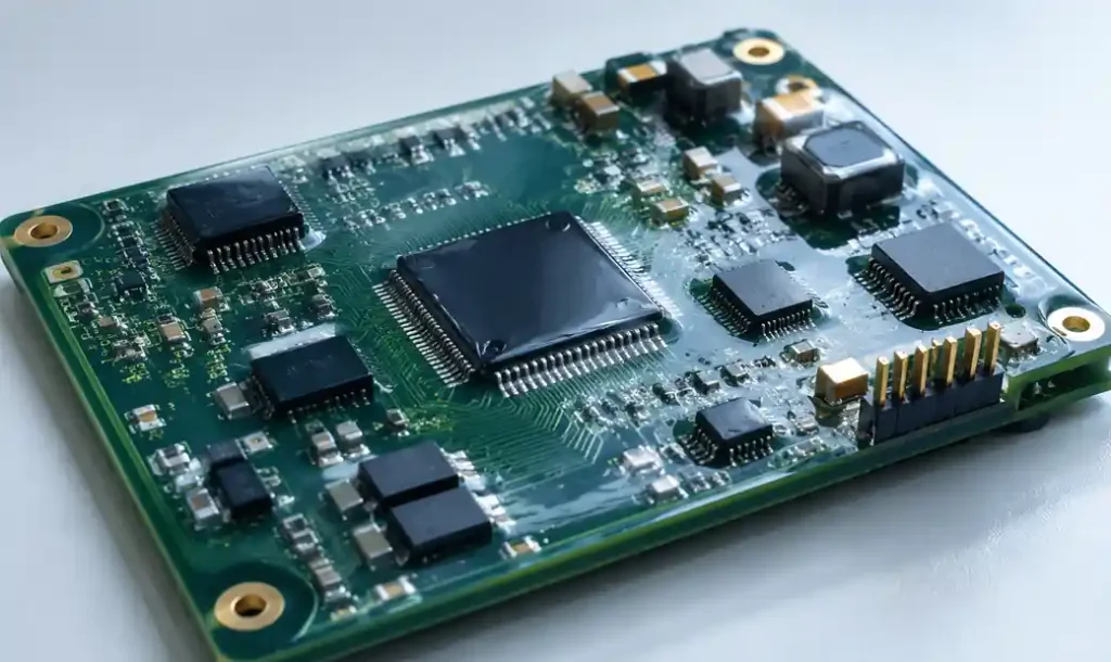
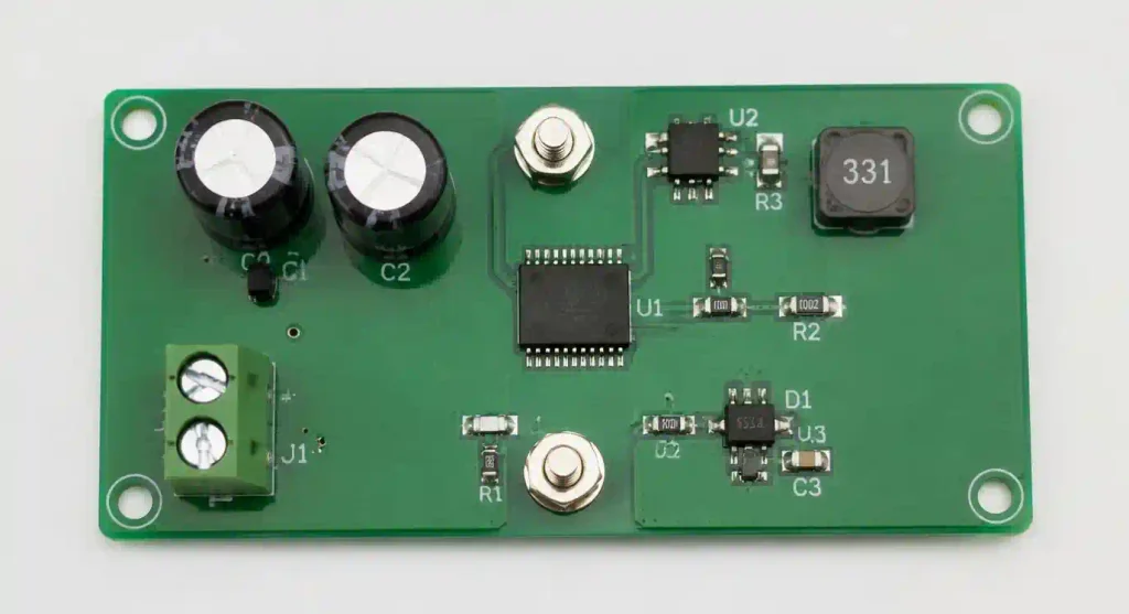
Component packages influence chemical resistance independent of substrate and coating choices. Plastic-encapsulated components absorb chemicals through epoxy molding compound, causing parameter drift or failure. Glass-sealed packages (ceramic or metal-can) eliminate this pathway but increase costs significantly.
Connector selection requires particular attention. Standard plastic connectors degrade when exposed to organic solvents, causing contact retention failures. Applications requiring reliable disconnection in chemical environments demand connectors with fluoropolymer or liquid crystal polymer housings and gold-plated contacts.
Component placement should minimize chemical trap points. Gaps between component bodies and PCB surfaces create capillary spaces that retain chemicals—maintaining prolonged contact with coated surfaces. Conformal coating penetration into these gaps is incomplete, leaving vulnerable areas. Designs should specify minimum 0.5mm clearance between component bodies and boards, filled by the coating process.
Via Protection and Sealing
Plated-through holes present chemical ingress pathways that coatings cannot fully seal. Standard conformal coating application leaves via barrels only partially filled—creating wicking channels for chemicals to penetrate through the board thickness.
Two approaches address this vulnerability. Via plugging with epoxy or solder mask ink seals holes before coating application. The process adds cost but eliminates through-board chemical migration. Alternatively, via tenting uses solder mask to cap holes on both sides, creating a sealed cavity. Testing shows plugged vias reduce through-board chemical penetration by 95% compared to unplugged holes with conformal coating alone.
Applications with extreme chemical exposure may require filled vias—where conductive or non-conductive epoxy completely fills the via barrel. This approach provides maximum protection but increases manufacturing cost and can affect via impedance in high-frequency designs.
Trace Width and Spacing Considerations
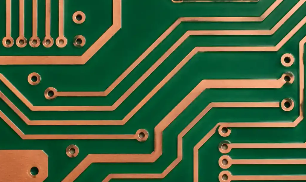
Chemical exposure increases the risk of electrochemical migration between adjacent conductors. Contaminants dissolved in moisture films create conductive paths between traces, causing intermittent shorts or leakage currents. Standard 0.15mm trace spacing provides minimal margin in chemically aggressive environments.
Designs for harsh chemical service should specify minimum 0.3mm conductor spacing—doubling the clearance available for migration paths to form. This conservative approach reduces leakage current risk and extends service life, particularly when ionic contaminants are present.
Trace width affects chemical attack vulnerability differently than spacing. Narrow traces etch completely through when exposed to acidic chemicals, creating open circuits. Wide traces survive longer, as partial etching still maintains continuity. Critical signal paths should use minimum 0.3mm trace widths even when circuit density would permit narrower conductors.
Testing and Qualification Protocols
Accelerated Chemical Exposure Testing
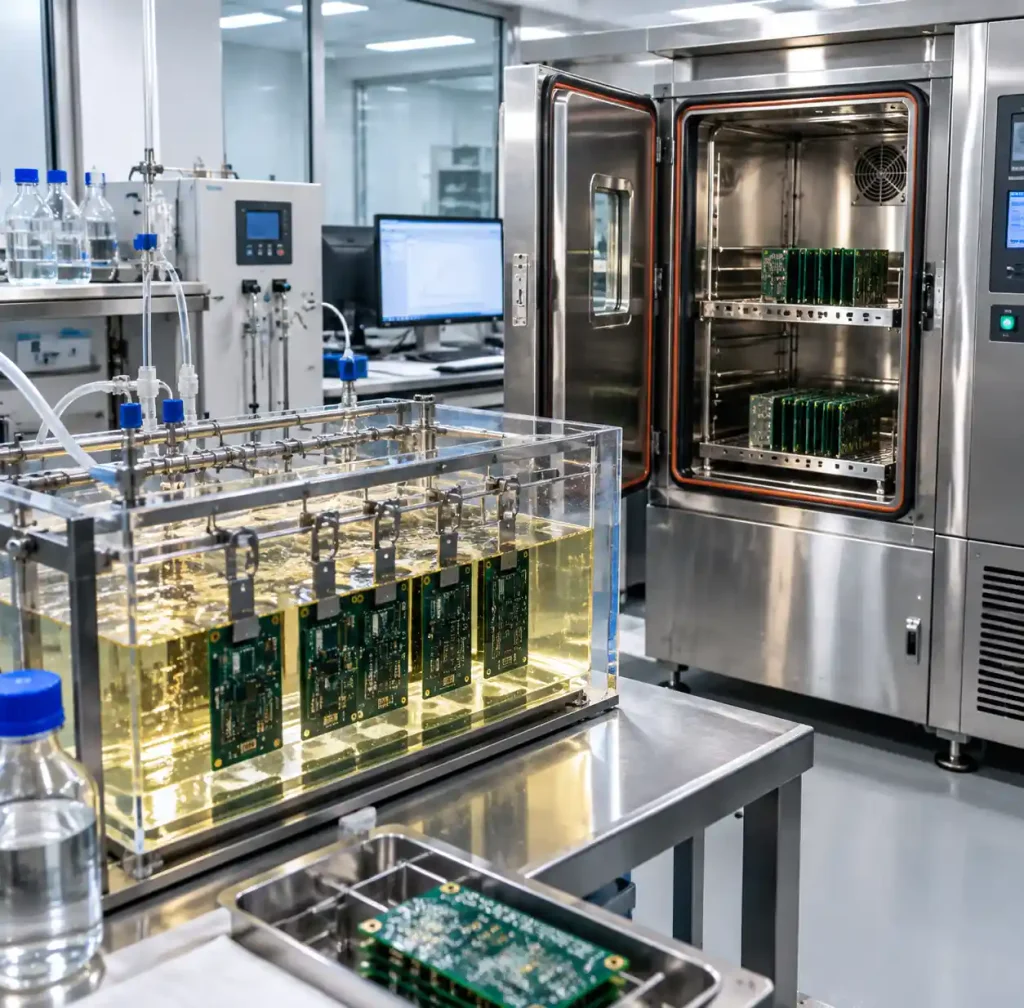
Laboratory testing compresses years of field exposure into weeks through elevated temperature and increased chemical concentration. Standard protocols immerse PCB samples in test chemicals at 60-80°C while monitoring electrical parameters at 24-hour intervals.
Insulation resistance between adjacent traces provides the most sensitive indicator of coating degradation. Resistance values below 100 MΩ at 100V DC indicate coating breakdown or chemical penetration. Testing continues until insulation resistance drops below 10 MΩ—defined as coating failure.
Temperature cycling combined with chemical exposure accelerates failure modes that develop slowly under constant conditions. Thermal expansion mismatch between substrate and coating creates microscopic cracks that provide chemical ingress pathways. Cycling between -40°C and 85°C in the presence of test chemicals reduces qualification time by 3-4 times compared to isothermal exposure.
Field Correlation and Validation
Accelerated test results require validation against actual deployment data. Chemical exposure in field environments is intermittent rather than continuous, and test chemical purity exceeds industrial process fluids. These differences mean laboratory predictions of service life are conservative.
One oil and gas equipment manufacturer found polyimide PCBs with urethane coating survived 4.2 years average service in drilling fluid exposure, while accelerated testing predicted 2.8 years. The discrepancy resulted from intermittent exposure patterns and drilling fluid additives that inhibited chemical attack. Correlation factors derived from field failures allow future designs to use accelerated testing with improved life predictions.
Material Selection Decision Framework
Cost-Performance Trade-offs
Material selection balances chemical resistance requirements against economic constraints. FR-4 substrates with acrylic coating cost $15-25 per square meter, while PTFE substrates with parylene coating exceed $200 per square meter. The 8-10x cost difference demands justification through extended service life or elimination of catastrophic failures.
Applications with mild chemical exposure (dilute acids, weak bases, aliphatic solvents) below 40°C rarely justify premium materials. FR-4 with urethane coating provides adequate protection at minimal cost. Field data shows 95% survival rates beyond 3 years in these conditions.
Moderate chemical environments (concentrated acids or bases, aromatic solvents, temperatures to 80°C) require polyimide substrates. Coating selection depends on specific chemicals present—urethane for oils and fuels, parylene for acids and bases. Cost increases 3-4 times over FR-4, but failure rates drop from 30% to under 5% over 5-year service periods.
Extreme environments (strong oxidizers, chlorinated solvents, temperatures exceeding 100°C) demand PTFE substrates with parylene coating. While costs are highest, these materials provide the only reliable solution. Alternative material combinations fail within months, making premium materials economically justified through elimination of replacement costs and downtime.
Application-Specific Guidelines
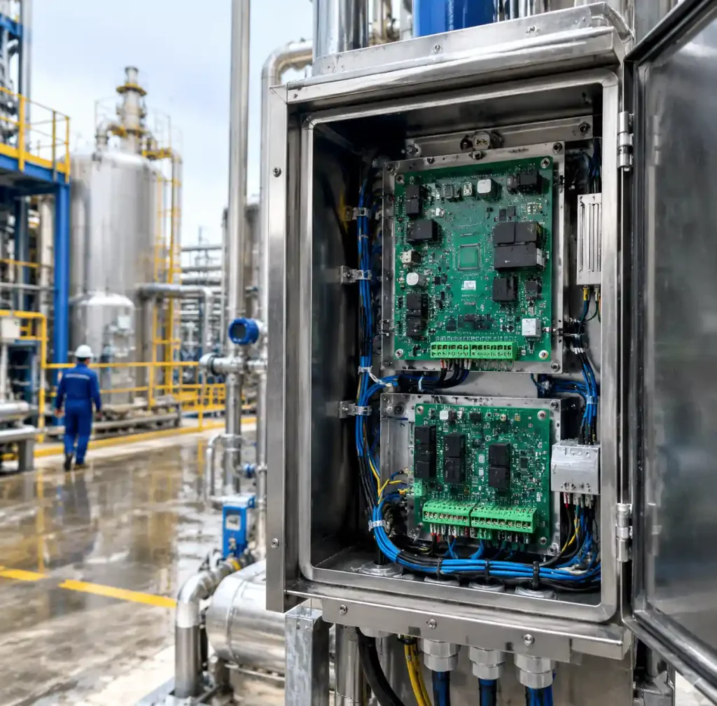
Chemical processing equipment operating in continuous exposure environments requires maximum protection. PTFE substrates with parylene coating should be specified as baseline, with glass-sealed components where possible. The harsh conditions accelerate any substrate or coating weakness, making premium materials essential for acceptable service life.
Industrial control panels located near chemical processes but not directly exposed need moderate protection. Polyimide substrates with urethane or silicone coatings balance protection against cost. Intermittent exposure patterns and lower chemical concentrations in panel environments allow these materials to achieve multi-year service life.
Portable instruments used in chemical facilities for periodic monitoring can use FR-4 substrates with robust coatings. Brief exposure durations during measurement cycles don’t challenge material limits. Urethane or parylene coatings provide adequate protection while containing costs for battery-powered devices replaced on 2-3 year cycles regardless of chemical exposure.
Frequently Asked Questions
What is the minimum coating thickness needed for chemical protection?
Coating thickness requirements vary by material type. Acrylic and silicone coatings need 50-75 microns minimum for adequate chemical barrier properties. Urethane coatings provide effective protection at 25-50 microns due to their denser polymer structure. Parylene coatings achieve excellent protection at just 10-25 microns thickness because of their pinhole-free deposition and low permeability. Thicker coatings don’t always improve protection—they can crack under thermal stress or create electrical clearance issues.
Can conformal coatings be applied over assembled components with plastic housings?
Yes, but coating compatibility with component plastics requires verification. Some conformal coating solvents attack polycarbonate and ABS component housings, causing stress cracking or crazing. Manufacturers provide compatibility charts listing safe combinations. When doubt exists, test samples should be coated and inspected for housing damage before production application. Alternatively, sensitive components can be masked during coating application, though this reduces protection and increases labor costs.
How does chemical exposure affect high-frequency PCB performance?
Chemical absorption in substrates changes their dielectric constant and loss tangent, shifting impedance and signal loss characteristics. FR-4 shows measurable changes in dielectric properties after absorbing 1-2% moisture or solvent by weight. PTFE substrates maintain stable electrical properties even after significant chemical exposure because fluoropolymers don’t absorb most chemicals. High-frequency designs operating above 1 GHz in chemical environments should specify PTFE-based laminates to prevent performance drift.
What cleaning processes are safe for chemically-resistant PCBs before coating?
Cleaning before coating application is critical but must avoid damaging substrate materials. Polyimide and PTFE substrates tolerate aggressive cleaning with isopropanol, acetone, or specialized flux removers without degradation. Standard aqueous cleaning with deionized water and mild detergents is safe for all substrate types. Avoid strong alkaline cleaners (pH > 12) on FR-4 boards, as these attack glass fibers and create surface roughness that reduces coating adhesion. After cleaning, boards must be thoroughly dried at 80-100°C to remove absorbed moisture before coating application.
Are there alternatives to parylene for maximum chemical protection at lower cost?
Two-layer coating systems provide improved protection approaching parylene performance at reduced cost. Applying a base layer of urethane (for chemical resistance) followed by a topcoat of silicone (for flexibility and additional barrier properties) creates a robust barrier. Testing shows this combination resists many aggressive chemicals for 2,000-3,000 hours—60-70% of parylene performance at about 40% of the cost. The approach works well for applications where parylene’s excellent but expensive protection exceeds requirements.
Conclusion
Reliable PCB operation in chemical environments demands careful material selection matched to exposure conditions. FR-4 substrates with acrylic coatings suit mild environments with occasional splash exposure. Polyimide substrates combined with urethane or parylene coatings protect against moderate chemical exposure and elevated temperatures. PTFE-based laminates with parylene coatings provide maximum protection for continuous immersion in aggressive chemicals.
Material costs scale with protection level—from $20 per square meter for FR-4 to over $200 for PTFE with parylene. However, extended service life and reduced failure rates justify premium materials in harsh environments. Accelerated testing protocols validated against field data allow engineers to predict service life and select materials meeting both technical and economic requirements. Proper design practices including component selection, via sealing, and conservative trace geometry enhance chemical resistance regardless of substrate and coating choices.
For applications requiring chemical protection beyond standard manufacturing capabilities, partner with a PCB manufacturer experienced in harsh environment designs. Andwin Circuits specializes in high-reliability PCB assemblies with comprehensive material selection, coating application, and qualification testing services.