
PCB for High-Altitude and Aerospace: Vacuum and Radiation Hardening
High-altitude and aerospace electronics face extreme challenges: ionizing radiation corrupting data, vacuum conditions causing material outgassing that contaminates optical systems, and temperature swings exceeding 200°C. For engineers designing satellite payloads, stratospheric UAVs, or deep-space missions, mastering vacuum behavior and radiation hardening determines mission success.
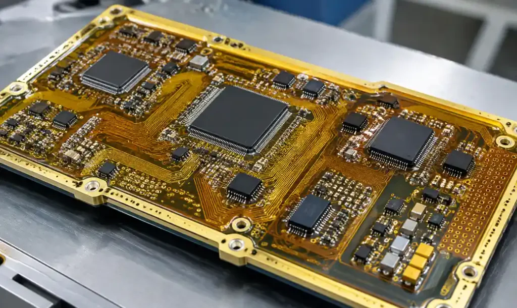
Vacuum Challenges: Material Outgassing Above 50,000 Feet
Above 15 kilometers, atmospheric pressure drops below 12 mbar, creating near-vacuum where conventional PCB materials release volatile organic compounds (VOCs). NASA’s ASTM E595 standard establishes acceptance thresholds: Total Mass Loss (TML) below 1.0% and Collected Volatile Condensable Materials (CVCM) below 0.1%.
Exceeding these limits causes outgassed molecules to migrate through vacuum, condense on optical lenses or solar cells, and permanently degrade performance. Engineers on the James Webb Space Telescope verified every PCB material through vacuum testing before flight qualification—standard FR-4 assemblies rarely pass.
Space-Grade Material Requirements
| Material Category | Standard Options | Space-Grade Alternatives | TML/CVCM |
|---|---|---|---|
| Substrate | FR-4 | Polyimide, Cyanate Ester | <0.5%/<0.05% |
| Solder Mask | Epoxy-based | Low-outgassing polyimide | <0.3%/<0.03% |
| Conformal Coating | Acrylic, Urethane | Parylene C, Silicone DC93-500 | <0.2%/<0.02% |
| Adhesives | Standard epoxy | Hysol EA9394 | <0.1%/<0.01% |
Polyimide substrates like Rogers ULTRALAM 3850HT deliver superior vacuum stability with glass transition temperatures exceeding 280°C. Similar principles apply to aerospace PCB assembly where material selection directly impacts reliability.
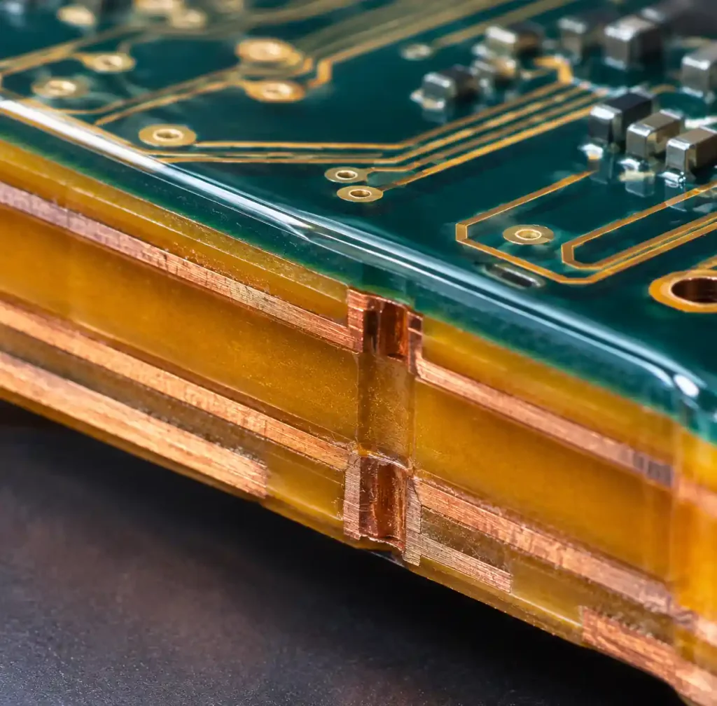
Radiation Hardening: Protecting Electronics from Invisible Threats
Aerospace electronics encounter three radiation threats: Total Ionizing Dose (TID), Single Event Effects (SEE), and displacement damage. In Low Earth Orbit, cumulative TID reaches 10-30 krad over 5 years. In Geostationary Orbit, that jumps to 100-300 krad—enough to destroy unhardened commercial electronics.
TID accumulates as ionizing particles create trapped charges in semiconductor oxides, shifting transistor threshold voltages. Single Event Effects strike when a heavy ion penetrates memory, flipping bits and corrupting data. On stratospheric UAVs above 60,000 feet, cosmic ray flux increases 100-fold compared to sea level.
PCB-Level Hardening Techniques
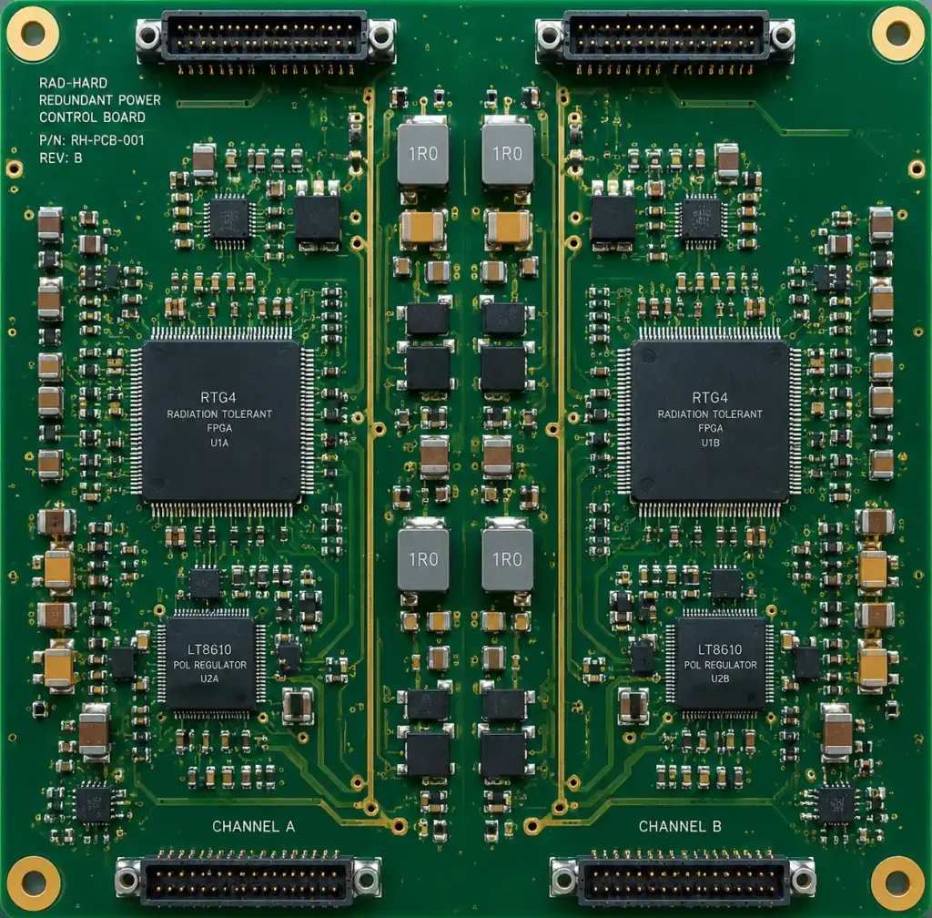
Triple Modular Redundancy (TMR)
Three identical circuit blocks on separate PCB regions process identical data. Majority voting circuits compare outputs and mask single-event upsets. NASA’s Mars Perseverance rover used TMR to reduce SEE-induced errors by 99.7% during its 7-month transit.
Strategic Shielding
Aluminum or tantalum shields between PCB layers attenuate low-energy particles. A 2mm aluminum shield reduces TID by 40% for energies below 1 MeV. The tradeoff: every millimeter adds 2.7 grams per square centimeter—critical when launch costs exceed $10,000 per kilogram.
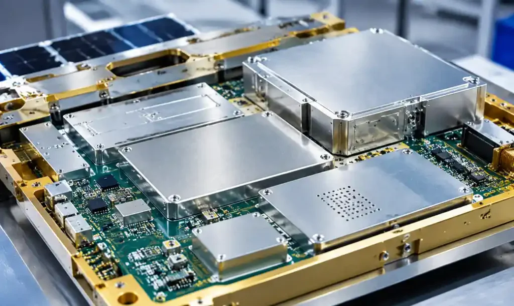
Component Placement
Position radiation-sensitive components behind structural elements. Mounting critical ICs under metal enclosures or battery packs reduces dose rates by 15-25% without dedicated shielding mass.
| Hardening Method | TID Protection | SEE Mitigation | Mass Penalty | Cost |
|---|---|---|---|---|
| TMR Circuit Design | Indirect | 99%+ | None | Medium |
| Aluminum Shield (2mm) | 40-60 krad | Low | 5.4 g/cm² | Low |
| Tantalum Shield (1mm) | 80-120 krad | Moderate | 16.7 g/cm² | High |
| Spot Shielding | 20-40 krad | Moderate | 1-3 g/cm² | Medium |
| EDAC + Scrubbing | N/A | High | None | Low |
Thermal Management in Vacuum: Redesigning Heat Dissipation
Earth-based electronics rely on convection for 60-80% of heat dissipation. In vacuum, only conduction and radiation remain. A 5W power IC may reach 180°C in orbit without redesigned thermal paths—exceeding the 125°C maximum junction temperature of most commercial components.
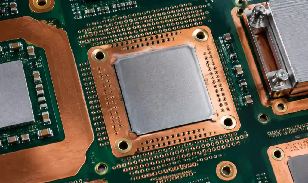
Wide copper pours (minimum 4oz weight) create low-resistance paths from heat sources to mounting surfaces. Thermal vias (0.3mm diameter, <1mm spacing) transfer heat through internal ground planes to chassis-mounted heat sinks. For aerospace grade PCBs, calculating via thermal resistance ensures adequate dissipation.
For a 1.6mm PCB with 20 thermal vias (0.3mm diameter), thermal resistance is approximately 8°C/W—sufficient for ICs dissipating up to 2W when coupled to aluminum chassis.
Radiative Cooling Enhancement
Emissivity coatings enhance radiative transfer. Black anodized aluminum (ε = 0.88) radiates 47% more energy than bare aluminum (ε = 0.09). On GEO satellites where sun-facing surfaces reach 120°C, high-emissivity coatings are mandatory.
Standards Compliance: Key Requirements
Aerospace PCBs must satisfy overlapping standards from NASA, ESA, military specifications, and IPC. Understanding which apply prevents costly redesigns during qualification.
IPC-6012 Class 3/A specifies space-grade acceptance: maximum 25μm hole wall roughness, ionic cleanliness <1.56 μg/cm² NaCl equivalent, and 100% automated optical inspection. NASA-STD-8739.4 covers crimping and termination requirements for edge connectors on deployable systems. ECSS-Q-ST-70-38C mandates X-ray inspection of solder joints exceeding 1.5mm diameter.

Case Study: Stratospheric Balloon Payload PCB
A university team designing a cosmic ray detector for 38 km altitude (8-hour duration) faced typical high-altitude challenges. Their initial FR-4 PCB with acrylic conformal coating failed vacuum testing.
Iteration 1: FR-4 substrate, acrylic coating → CVCM 0.18% (failed)
Iteration 2: Polyimide substrate, silicone coating → CVCM 0.09% (marginal)
Iteration 3: Cyanate ester substrate, Parylene C coating → CVCM 0.03% (passed with margin)
The team implemented Error Detection and Correction (EDAC) in their FPGA—during flight, EDAC corrected 23 single-bit upsets over 8 hours, validating soft-error mitigation even for sub-orbital missions.
Advanced Techniques
Additive Manufacturing for Shielding
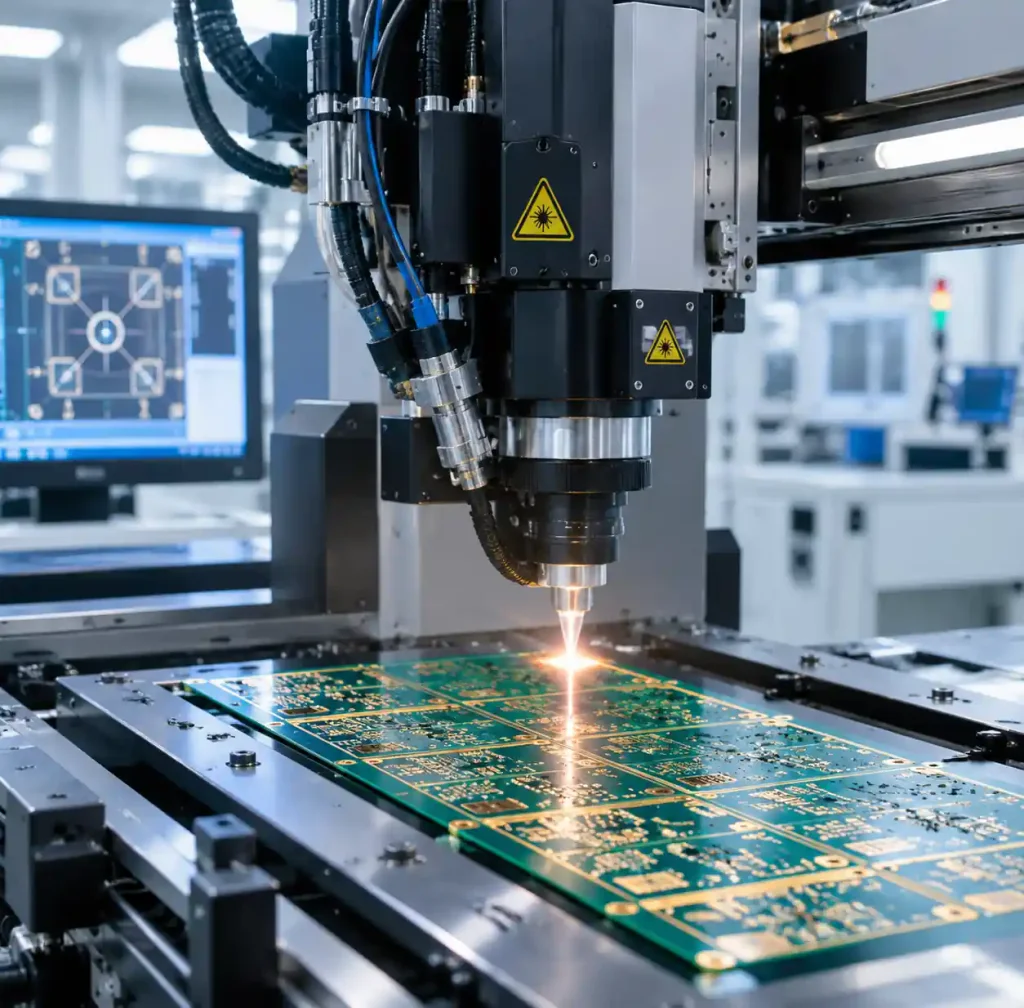
Aerosol jet printing allows direct deposition of tungsten-doped polymer shields onto PCB surfaces. Demonstrated by JPL for Mars 2020, this reduces shielding mass by 40% compared to mechanically attached plates.
Self-Healing Circuits
Emerging research incorporates phase-change materials that automatically reroute current after radiation-induced short circuits. While in laboratory testing, this could extend mission lifetimes in high-radiation environments like Jupiter orbit, where TID exceeds 1 Mrad annually.
Design Verification Checklist
Before prototype fabrication, verify:
✓ All materials pass ASTM E595 (TML <1.0%, CVCM <0.1%)
✓ Thermal vias under power components (8 vias per watt minimum)
✓ Copper weight ≥2oz on internal power planes
✓ Trace spacing ≥3W for impedance-controlled signals
✓ EDAC implementation on memory >1 Mb
✓ Watchdog timers with radiation-hard oscillators
✓ SEE-sensitive ICs placed under passive shielding
✓ Ground plane continuity verified
✓ Conformal coating thickness 50-75μm
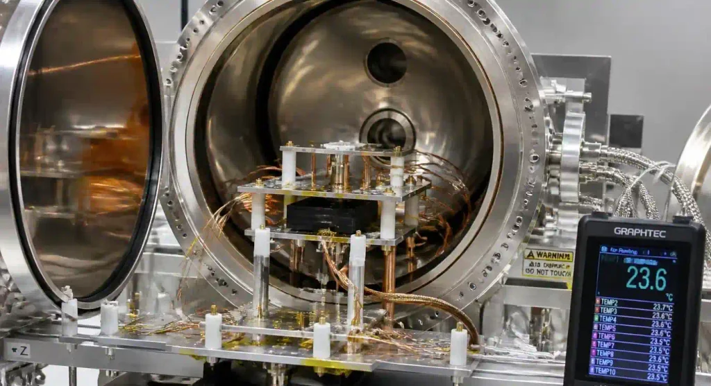
✓ Thermal vacuum bake-out testing (125°C, 24h)
Cost vs. Reliability Tradeoffs
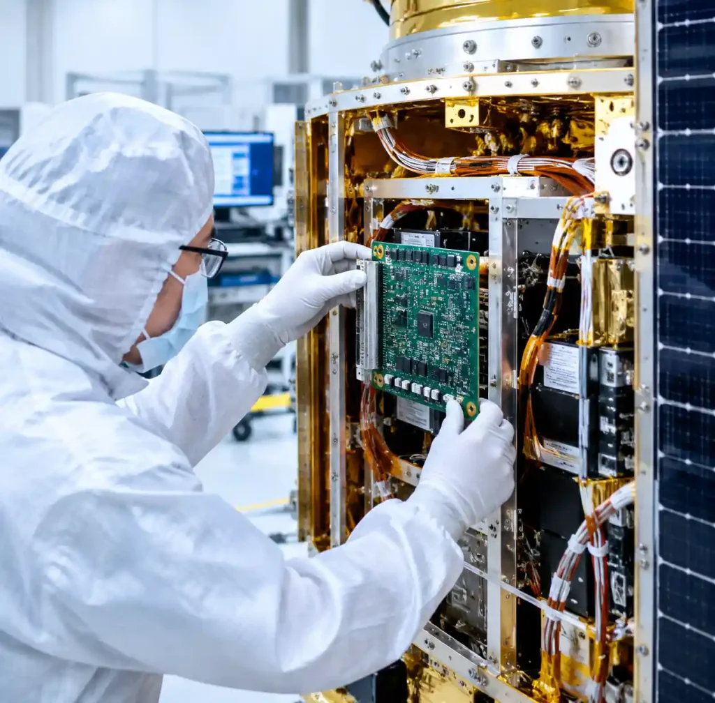
Full space-grade qualification costs $80,000-$250,000, including radiation testing at cyclotron facilities and thermal vacuum cycling per NASA-STD-7001A. For stratospheric balloons or short-duration UAV flights, COTS components with selective hardening reduce costs to $15,000-$40,000.
| Mission Duration | Radiation Dose | Recommended Approach | Typical Cost |
|---|---|---|---|
| <24 hours | 0.01-0.05 krad | COTS + EDAC + selective TMR | $15-30K |
| 1-3 years (LEO) | 5-20 krad | Rad-tolerant + shielding | $80-150K |
| 5-10 years (GEO) | 50-200 krad | Rad-hard + TMR + shielding | $200-500K |
| >10 years (deep space) | >500 krad | Full rad-hard redundant | $1-5M |
FAQ
Can FR-4 PCBs survive in space for short missions?
Standard FR-4 functions in vacuum for missions under 6 months if conformal coating passes ASTM E595. However, temperature cycling performance suffers—polyimide or cyanate ester substrates provide better thermal reliability over repeated -100°C to +100°C cycles.
How much radiation shielding is needed for LEO satellites?
For 5-year LEO missions, 2mm aluminum provides baseline protection for CMOS electronics rated to 50 krad. Critical components like FPGAs and SRAM require additional spot shielding (1mm tantalum) or radiation-hardened alternatives.
What’s the practical altitude limit for unpressurized PCB operation?
Unpressurized PCBs with proper materials reliably operate to 40 km. Above this, corona discharge becomes problematic at high voltages (>50V), requiring increased creepage distances or voltage derating.
Do all aerospace PCBs need IPC Class 3 qualification?
Mission criticality determines requirements. Human-rated spacecraft mandate Class 3/A. Expendable launchers often use Class 3. Commercial CubeSats may accept Class 2 with enhanced inspection—reducing costs 30-40% compared to full Class 3.
How long does radiation testing take?
TID testing spans 2-4 weeks for dose accumulation. SEE characterization requires 1-2 weeks at heavy-ion facilities. Total qualification including documentation: 3-6 months.
Can consumer-grade components work in stratospheric applications?
Selectively, yes. Many modern SoCs with built-in ECC survive single-flight balloon missions. The risk: unknown radiation sensitivity and limited temperature range. Budget 20% excess payload capacity for failures.
Conclusion
Designing PCBs for high-altitude and aerospace environments demands rigorous attention to vacuum compatibility and radiation hardening. Material selection drives vacuum performance—polyimide or cyanate ester substrates with low-outgassing coatings meet ASTM E595 thresholds that FR-4 cannot achieve. Radiation hardening requires layered defense: TMR, strategic shielding, and EDAC working together to maintain data integrity under particle bombardment.
The cost-to-reliability spectrum spans three orders of magnitude, from $15K balloon payloads using COTS-with-mitigation to $5M deep-space systems built entirely from rad-hard components. Understanding mission-specific radiation dose, duration, and acceptable failure rates guides economically rational design decisions. As launch costs decline, engineering practices proven on flagship NASA programs are becoming baseline for commercial satellite constellations and stratospheric platforms.