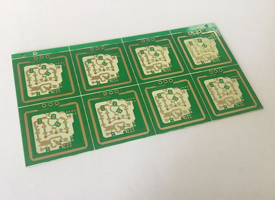
Selective hard gold plating pcb manufacturing
What is selective hard gold plating pcb?
Selective hard gold plating pcb is selective plating a part area of PCB,
with thick nickel and hard gold,
Other area of PCB with normal surface finishing ( Immersiong gold,OSP or HASL).
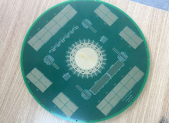
Selective hard gold plating pcb’s Application
The Selective hard gold plating pcb with better abrasive resistance,low contact resistance,
It widely used in products which have key and contact positions increase the wear resistance
And electrical conductivity,such as,hard disk, internal memory and motor Etc..
How to make Selective hard gold plating pcb?
Because only a part of area need to be hard Gold plating PCB,and it need to do as special PCB manufacturing process,
There are 2 ways to finish the gold plating to selective.
1.No bus bar electronic plating.
A> For example,if customer’s requirement:
Selective hard gold plating( Au: > 3 U”) + Normal Gold plating ( 0.5 – 3 U”)
Then,the PCB manufacturing process is :
Front Process -> drill -> PTH ->Plating copper -> Circuit Figure (1) -> Plateing Gold(Normal thickness) ->
Circuit Figure (1)(Only Selective hard gold plating area)-> hard Gold palting -> other
2.Automatic Optic Inspection (A.O.I)
AOI device is for inspection the compoents placement and solder joint quality after SMT(Surface Mounted Technology).
To achieve better quality control,find and remove the errors early in the assembly process.
It is avoid the defective product to assembly,will avoid scrapping the repairable circuit board.
3.X-Ray inspection
X-ray is a very short wavelength of electromagnetic waves, the wavelength range of 0.0006 a 80nm,
with a strong penetration,X-ray could penetrate a variety of different density of the material.
When the design have BGA or QFN,for checking the solder quality that could not be visible by eyes.
We will use X-ray machine to inspect the BGA or QFN package in finished PCB assembly.
4.Final Quality Assuerance (FQA)
After all the above quality control processes,
Quality Engineer will make final quality visual inspection for the all product.
5.Functional Test
Functional Test are based on automated test tools to simulate a variety of normal, peak and abnormal load
conditions to test the performance of the final PCB assembly products.
Functional Test is a complex process,which include Tool made,Programming and testing,
need technicality support from customer.
What industry we serve?


High Precision onestop turnkey PCB Assembly Services
Contact our team today Email: sales@andwinpcb.com
Or fill follow form,we will contact you soonest