What id the potential for high-frequency application of PCB-wound transformers?
PCB-wound transformer are a new type of transformer manufactured using printed circuit board(PCB)technology.

PCB-wound transformer are a new type of transformer manufactured using printed circuit board(PCB)technology.
PCBs are widely used in China.The manufacturing process generates contaminants,including residual flux and adhesives,dust,and debris from the manufacturing process.If the PCB surface is not effectively cleaned,resistance and leakage can lead to PCB failure,thus shortening the product’s lifespan.Therefore,cleaning PCBs is a crucial step in the manufacturing process 1.Semi-aqueous cleaning primarily uses a cleaning agent composed of…
With the booming PCB industry ,more and more engineers and technicians are joining the ranks of PCB design and manufacturing.However,due to the wide range of areas involved in PCB manufacturing,and the fact that a significant number of PCB design engineers(layout personnel)have no experience in or involvement in PCB manufacturing,and the fact that a significant number…
When a design has very high thermal dissipation requirements ,using an aluminum-based pcb is a very effective solution.This design is able to better transfer heat energy away from the design component,thereby controlling the project’s temperature.It is often ten times more efficient at removing heat from circuit component than an equivalent fiberglass backing.This significantly higher level…
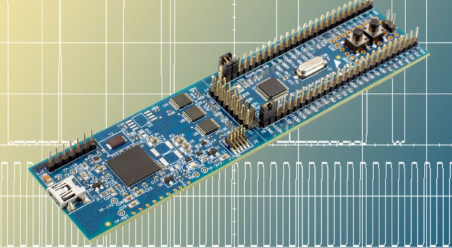
PCB(printed circuit board) are key supporting structures for electronic components,connecting them with metal conductors to enable the functionality of various electronic devices.In the early 20th century,traditional PCB manufacturing primarily involved printing each resist.However,with the rapid advancement of semiconductor technology, the demand for PCBs has skyrocketed. Modern PCBs have evolved from single-sided boards to double-sided boards,…
Although current EDA tools are powerful,PCB design remains challenging as PCB dimensions shrink and device density increases.How can we achieve high PCB routing yields and shorten design time?This article introduces design techniques and key points for PCB planning layout,and routing.While PCB design time is shrinking,shrinking board space,increasing device density,extremely stringent layout rules,and large component are…
At work, I ensure that assembled PCBs avoid these types of errors. With hundreds of tiny components soldered onto them, PCBs are less robust than you might imagine. If handled improperly, you risk complaints from unhappy system installers whose circuits may not function properly. Should PCB Designers Be Concerned About PCB Handling? Odds are, you’re…
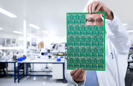
PCBs (printed circuit boards) are an indispensable component of electronic devices, and their quality and accuracy have a crucial impact on the performance and lifespan of the entire device. Optical positioning is a key technology in the PCB production process, crucial for ensuring PCB accuracy and consistency. This article will discuss the requirements for PCB…
PCB design has become increasingly complex as the complexity of the devices they carry increases.For a long time,circuit designers have worked in isolation,then then transferred the completed schematics to PCB designers.PCB designers the completed their work independently and transferred the Gerber files to the PCB fabricator.These three groups worked in isolation,with lilttle communication. With the…
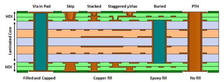
Vias are a crucial component of multilayer PCBs, and drilling costs typically account for 30% to 40% of the overall PCB fabrication cost. Simply put, every hole on a PCB can be called a via. Based on their function, vias can be categorized into two types: one for electrical connection between layers; the other for…
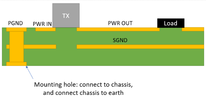
In PCB design, grounding is a crucial measure for suppressing noise and preventing interference. Different grounding methods are used depending on the circuit. Only proper grounding can reduce or avoid mutual interference between circuits. There are two main grounding methods in daily life: single-point grounding and multi-point grounding. This article will focus on how to…
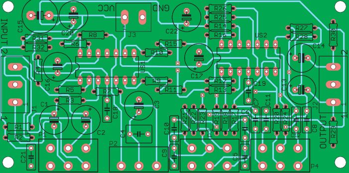
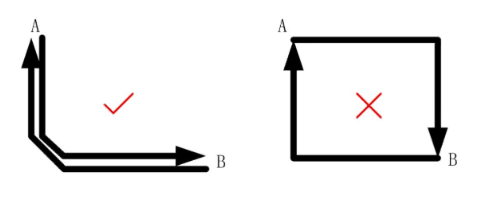
IN PCB design,routing is a crucial step in completing a product design.It’s a process that demands the most attention,requires the most skill,and requires the most effort.PCB routing can be performed in single-sided,double sided,or multi-layer configurations,There are two routing methods;automatic routing and interactive routing.Before automatic routing and interactive routing.Before automatic routing and interactive routing.Before automatic routing,interactive…
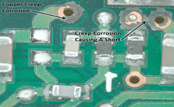
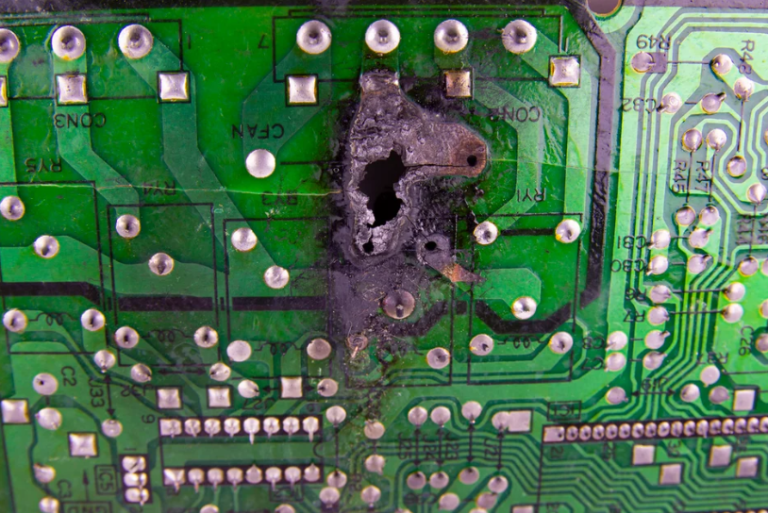
Excessive corrosion of pcb is a serious problem that can lead to short circuits,reduced current capacity,increased resistance,and even affect the overall performance and lifespan of the device.To prevent this,multiple aspects must be addressed,including design,material selection,manufacturing process,storage environment,and maintenance.The following will discuss in detail strategies for effectively preventing excessive pcb corrosion 1.Preventive Measure During the design…
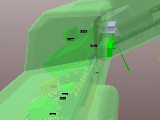
Designing printed circuit boards (PCBs) is both fun and challenging, but PCBs require enclosures for mechanical stability. PCB enclosures can be purchased off-the-shelf or custom designed using MCAD tools. Regardless of the method chosen to create the enclosure, the PCB layout must be imported into the MCAD tool to ensure that the board and components…
The global HDI printed circuit board market is projected to reach $24.63 billion by 2025, achieving a compound annual growth rate of 12.8%. Factors such as the increasing miniaturization of electronic devices, the rapid consumer adoption of smart devices, the significant growth of consumer electronics, and the increasing adoption of automotive safety measures are driving…
We use cookies to improve your experience on our site. By using our site, you consent to cookies.
Manage your cookie preferences below:
Essential cookies enable basic functions and are necessary for the proper function of the website.
Statistics cookies collect information anonymously. This information helps us understand how visitors use our website.
Google Analytics is a powerful tool that tracks and analyzes website traffic for informed marketing decisions.
Service URL: policies.google.com (opens in a new window)
SourceBuster is used by WooCommerce for order attribution based on user source.
You can find more information in our privacy policy and privacy policy.