Revealing the design requirements of RF PCB and the application of laser soldering
In today’s era of rapid development of electronic technology, the design and welding technology of RF PCB circuit boards are…
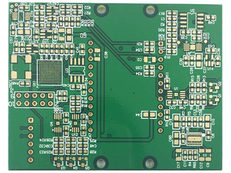
pcb design
In today’s era of rapid development of electronic technology, the design and welding technology of RF PCB circuit boards are…
Introduction to PCB Layout Tools Printed Circuit Board (PCB) layout tools are specialized software applications that enable engineers and designers…
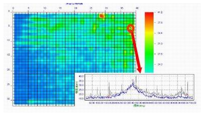
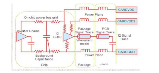
Traditional tools for debugging PCB include: time domain oscilloscope, TDR (time domain reflectometry) oscilloscope, logic analyzer, and frequency domain spectrum…
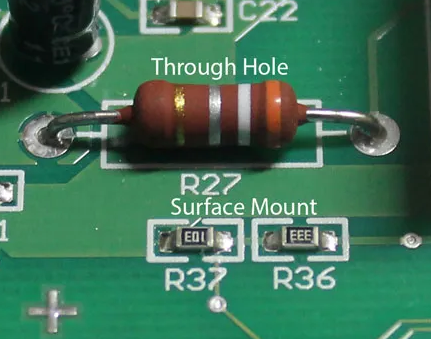
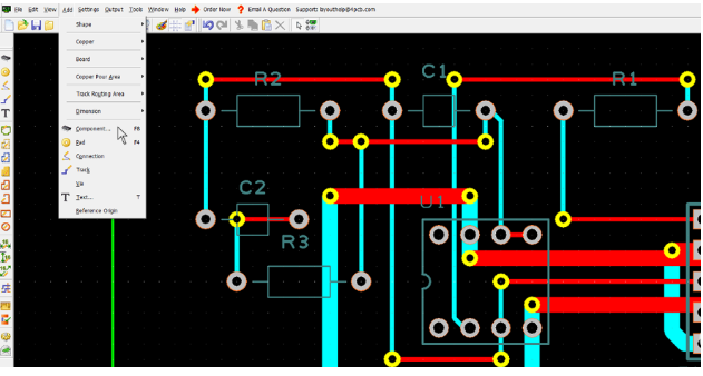
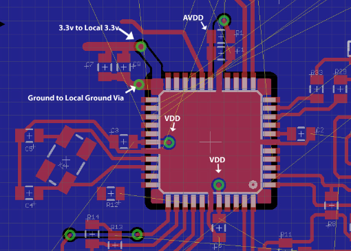
1.Consider the choice of component package Throughout the schematic drawing stage, you should consider the component package and land pattern…
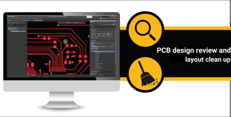
1.Selection of proofing method PCB proofing can be divided into three methods, namely regular PCB factories, professional sample companies and…
In electronic design, after the project schematic design is completed and compiled, the PCB design needs to be carried out….
Introduction In the realm of electronic design, the terms “layout” and “PCB” (Printed Circuit Board) are intimately connected, representing two…
In Altium Designer (AD for short), associating schematics with PCBs is an important design step that ensures a smooth transition…
After the PCB design is completed, we need to perform functional checks on all projects. Just like when we finish…
Introduction Crystal oscillators serve as the heartbeat of modern electronic systems, providing precise timing references for microcontrollers, processors, and communication…
Abstract This paper presents a comprehensive design approach for a printed circuit board (PCB) that monitors heart rate during physical…

Introduction Printed Circuit Board (PCB) design has evolved significantly from its purely functional origins. Today, PCB designers increasingly incorporate graphical…
Abstract Printed Circuit Board (PCB) design and manufacturing rely heavily on visual inspection and computer-aided design tools. The highlight display…
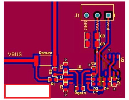
I have written several articles about Buck and Boost, but PCB layout is rarely mentioned. This article will talk about…
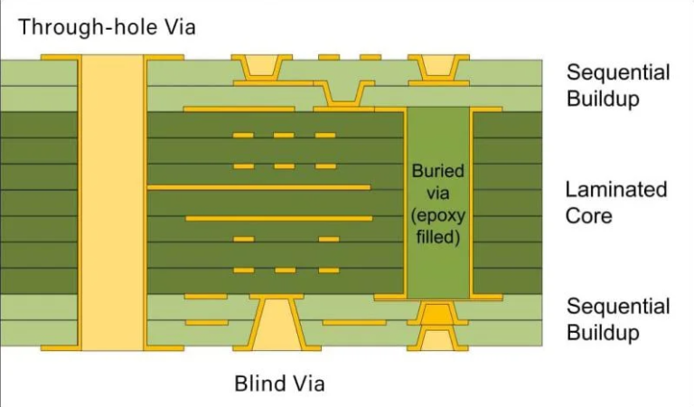
Abstract Blind vias are essential in modern high-density printed circuit board (PCB) designs, enabling connections between outer layers and inner…
We use cookies to improve your experience on our site. By using our site, you consent to cookies.
Manage your cookie preferences below:
Essential cookies enable basic functions and are necessary for the proper function of the website.
Statistics cookies collect information anonymously. This information helps us understand how visitors use our website.
Google Analytics is a powerful tool that tracks and analyzes website traffic for informed marketing decisions.
Service URL: policies.google.com (opens in a new window)
SourceBuster is used by WooCommerce for order attribution based on user source.
You can find more information in our privacy policy and privacy policy.