What are the basic manufacturing and process requirements of PCB
1. Basic PCB manufacturing
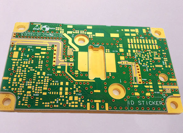
The Chinese name of PCB is “circuit board” target=”_blank”>Printed circuit board, also known as printed circuit board, is an important electronic component. So what is the basic process flow of PCB production? The following editor will guide you Learn about.
The basic process flow of PCB production is mainly: inner circuit → lamination → drilling → hole metallization → outer dry film → outer layer circuit → silk screen → surface process → post-process
Inner layer circuit: The main process is cutting → pre-processing → lamination → exposure → DES → punching.
Lamination: Laminate copper foil, prepreg and browned inner circuit board into a multi-layer board.
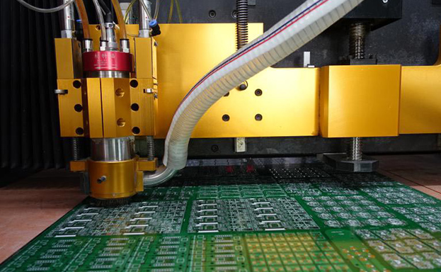
Drilling: Create through holes between the layers of PCB to connect the layers.
Hole metallization: Metalizing the non-conductive part of the hole wall can make the subsequent electroplating process more convenient. If you are making a multi-layer PCB board and it contains buried holes or blind holes, each layer of the board must be drilled and electroplated before bonding. If you don’t go through this step, there will be no way to connect to each other. After drilling by machine equipment according to drilling requirements, the inside of the hole must be electroplated (Plated-Through-Hole technology, PTH). After metal treatment is performed on the inside of the hole wall, the internal layers of circuits can be connected to each other. Before starting plating, the holes must be cleared of debris. This is because the resin epoxy will produce some chemical changes after heating, and it will cover the internal PCB layer, so it must be cleaned off first. Both cleaning and plating actions are completed during the chemical process.
Outer dry film: The required lines are exposed on the dry film through pattern transfer technology.
Outer layer circuit: The purpose is to plate the copper thickness to the thickness required by the customer and complete the circuit shape required by the customer.
Silk screen: The protective layer of the outer circuit, used to ensure the insulation, protection board and solder mask of the PCB.
Post-processing: Complete processing according to customer requirements and conduct testing to ensure final quality audit. Both THT and SMT parts are installed and placed on the PCB using machinery and equipment.
THT parts are usually soldered using a method called wave soldering. This allows all parts to be soldered to the PCB at once. Start by cutting the pins close to the board and bending them slightly to allow the parts to hold. Then move the PCB to the water wave of the cosolvent, allowing the bottom to contact the cosolvent, so that the oxides on the bottom metal can be removed. After heating the PCB, this time moving it over to the molten solder, the soldering is complete once it makes contact with the bottom.
The method of automatically welding SMT parts is called Over Reflow Soldering. The paste solder containing flux and solder is processed once after the part is installed on the PCB, and again after the PCB is heated. After the PCB has cooled and the soldering is complete, the next step is to prepare the PCB for final testing.
2. PCB processing technology requirements
1. Number
After PCB processing is completed, it should be uniformly numbered immediately. In order to prevent the marks from being lost during processing and cleaning, a unified number should be clearly written on both sides of the board with a marker. For future management convenience, this number should be retained permanently.
2. Place it correctly
In order to minimize bumps and scratches on the surface of components, during the processing, transportation, and storage of PCBs, care must be taken to handle them with care to prevent bumps, and boards also need to be separated and stacked to avoid Contact each other, causing PCB boards to damage each other.
3. Post-finishing process of PCB processing
After the PCB is processed and tested, it is necessary to perform post-finishing work on the entire board, including removing excess items on the surface such as excessive pins and metal residues; beautifying the finished product after PCB processing, such as as much as possible The flying wires on the front should be concealed; for the flying wires on the back, it can be as little as possible, and it is best to take shortcuts; and the solder joints and longer flying wires should be covered and fixed with the minimum amount of glass glue so that they will not affect the Beautiful exterior. Because for a first-class PCB processing manufacturer, both internal and external aspects are equally important; therefore, redundant marks must be removed, the color must be consistent, and the PCB board must be kept clean. If it is stained with dirt, use a brush or Cotton ball cleaning.
After each PCB is processed, it must go through tedious sorting work before it can be packaged. The finished product received by each consumer has gone through countless processes and cannot have any errors. Every honest and reliable PCB processing manufacturer strictly implements the above process and is constantly striving for excellence, only to become more professional and to bring more affordable PCB processing products to consumers who trust it.