
X-ray Inspection for PCB: BGA Void Analysis and Hidden Defect Detection
When a $2.3M automotive radar production run failed thermal cycling at -40°C, the root cause traced back to 32% voiding in BGA thermal pads—visible only through X-ray inspection. The boards passed AOI and flying probe testing but solder voids created thermal hot spots that triggered failures under load, costing six weeks of rework and damaging customer confidence.
X-ray inspection reveals hidden structures inside PCB assemblies—BGA solder joints, buried vias, inner layer traces, and thermal interfaces that optical methods cannot reach. For high-reliability electronics, X-ray verifies structural integrity before boards reach the field.
Why X-ray Inspection Matters for Modern PCB Assembly
Optical inspection sees surfaces. X-ray sees through them. As packages shrink and layer counts rise, critical joints hide beneath components or inside multilayer stackups.
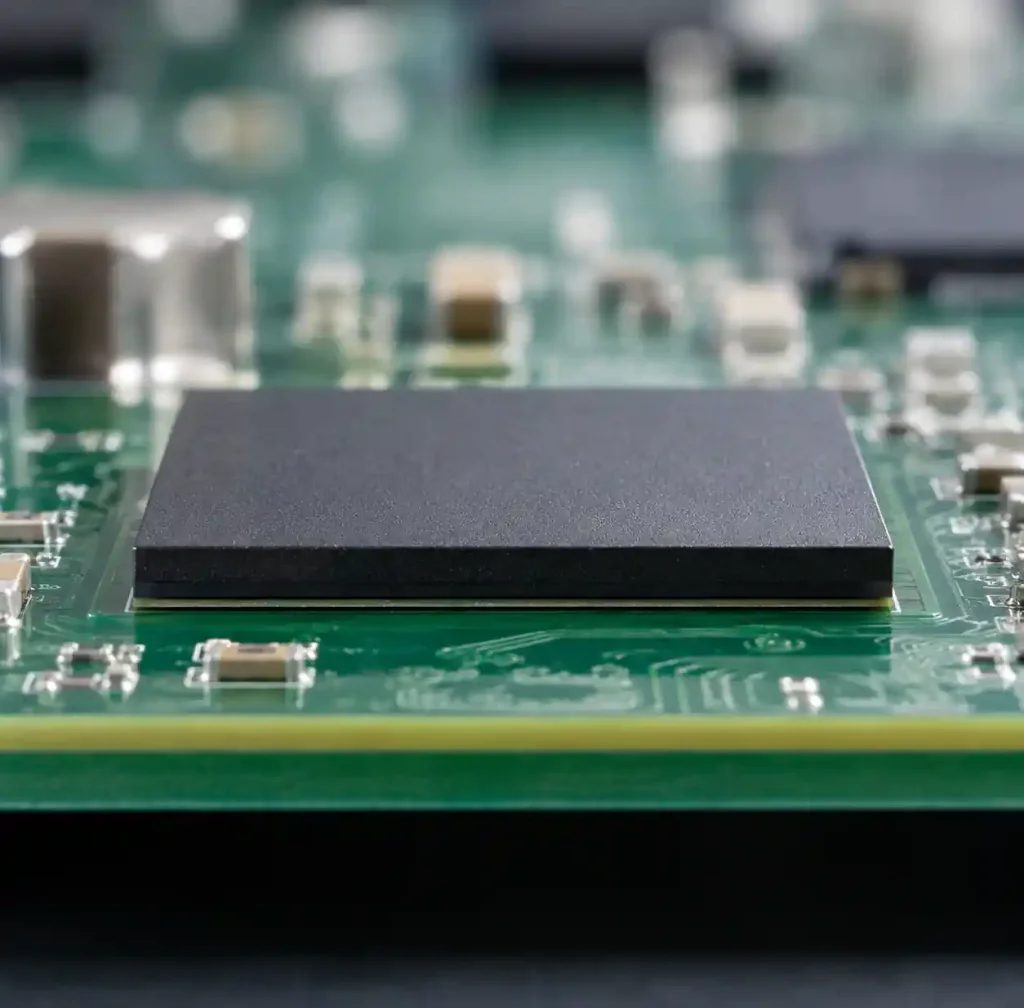
BGA packages dominate high-performance designs—processors, FPGAs, power management ICs. Every solder ball sits hidden under the package body. QFN packages with exposed thermal pads present similar challenges: the primary thermal connection lives underneath, inaccessible to optical inspection.
HDI boards with blind and buried vias bury connections inside the stackup. A 0.1mm microvia with inadequate plating creates high resistance that degrades signal integrity or fails under thermal stress. Inner layer defects—incomplete etching, registration errors, lamination voids—remain invisible until X-ray exposes them.
X-ray Imaging Physics: How It Detects Hidden Defects
X-ray inspection works through differential absorption. Different materials absorb radiation at different rates based on density. Solder appears bright white due to high absorption. FR-4 substrate and component bodies appear gray. Air voids appear black—they absorb almost nothing.
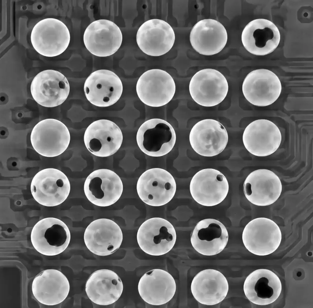
This contrast makes voids immediately visible as dark regions within bright solder joints. Systems operate at 20-160kV accelerating voltage. Lower voltages provide better contrast for thin assemblies but struggle with thick boards. Higher voltages penetrate multilayer boards but reduce fine feature contrast. Modern microfocus X-ray tubes with 1-3 micron spot sizes enable detailed void analysis with resolution below 10 microns.
2D X-ray vs 3D X-ray Systems
2D X-ray produces transmission images showing all features projected onto one plane. This works for simple assemblies but complex multilayer assemblies create overlapping features. 3D X-ray systems reconstruct volumes from multiple projections using CT or laminography.
| Feature | 2D X-ray | 3D CT | 3D Laminography |
|---|---|---|---|
| Image clarity | Overlapping features | Full 3D volume | Single plane focus |
| Inspection time | 5-30 seconds | 3-15 minutes | 45-90 seconds |
| Void accuracy | ±5-10% | ±1-2% | ±2-4% |
| Best use | Single-sided screening | Failure analysis | Production double-sided |
| Cost | $80K-150K | $400K-800K | $250K-450K |
Laminography reconstructs a single plane in sharp focus while blurring out-of-plane features, eliminating confusion from overlapping components with <90 second cycle times. CT provides complete data but requires 5-15 minutes per board, limiting use to failure analysis.
BGA Void Analysis: IPC Standards and Acceptance Criteria
Voids degrade electrical and thermal performance. Electrically, voids increase resistance and create current density hot spots. Thermally, voids block heat conduction—air conducts heat roughly 1/1000th as effectively as solder.
IPC-A-610 Class 3 allows maximum 25% voiding by area per ball. IPC-7095D provides detailed guidance: 25% total void area, no single void exceeding 50% of ball diameter, maximum three voids per ball.
| IPC Class | Max Void % | Max Single Void | Max Voids/Ball | Application |
|---|---|---|---|---|
| Class 1 | No limit | No limit | No limit | Consumer electronics |
| Class 2 | 30% | No limit | No limit | Industrial |
| Class 3 | 25% | 50% of diameter | 3 | Aerospace, medical, automotive |
These standards address reliability but don’t account for thermal performance. For power devices dissipating >2W, stricter limits apply: 15% maximum in central thermal pad region. A 10×10mm pad with 20% voiding adds 4-6°C/W thermal resistance. For a 15W power amplifier, this represents 60-90°C additional junction temperature rise.
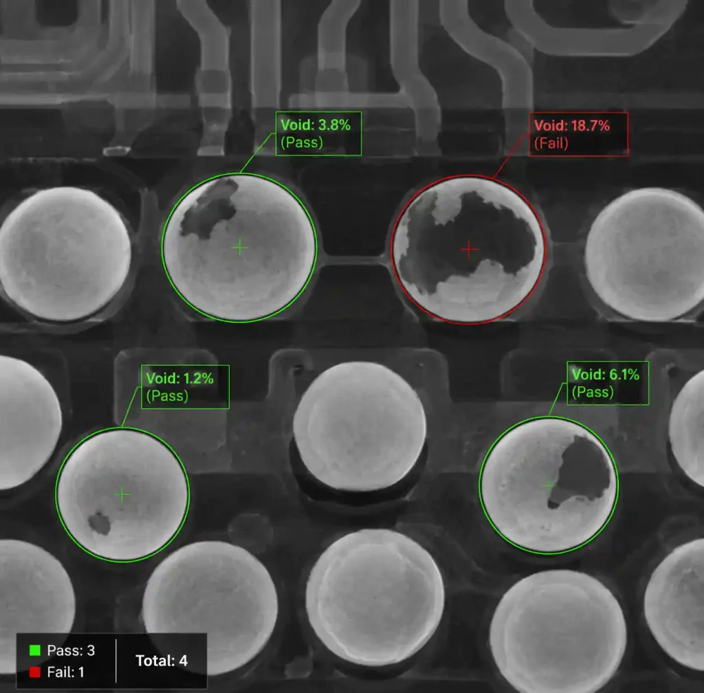
Void location matters more than percentage. Central voids directly block the heat path. Peripheral voids have less impact. Automated algorithms calculate total percentage but don’t weight location properly—manual review remains necessary for thermal-critical components.
Hidden Defects X-ray Reveals Beyond BGA Voids
X-ray catches defects invisible to optical methods:
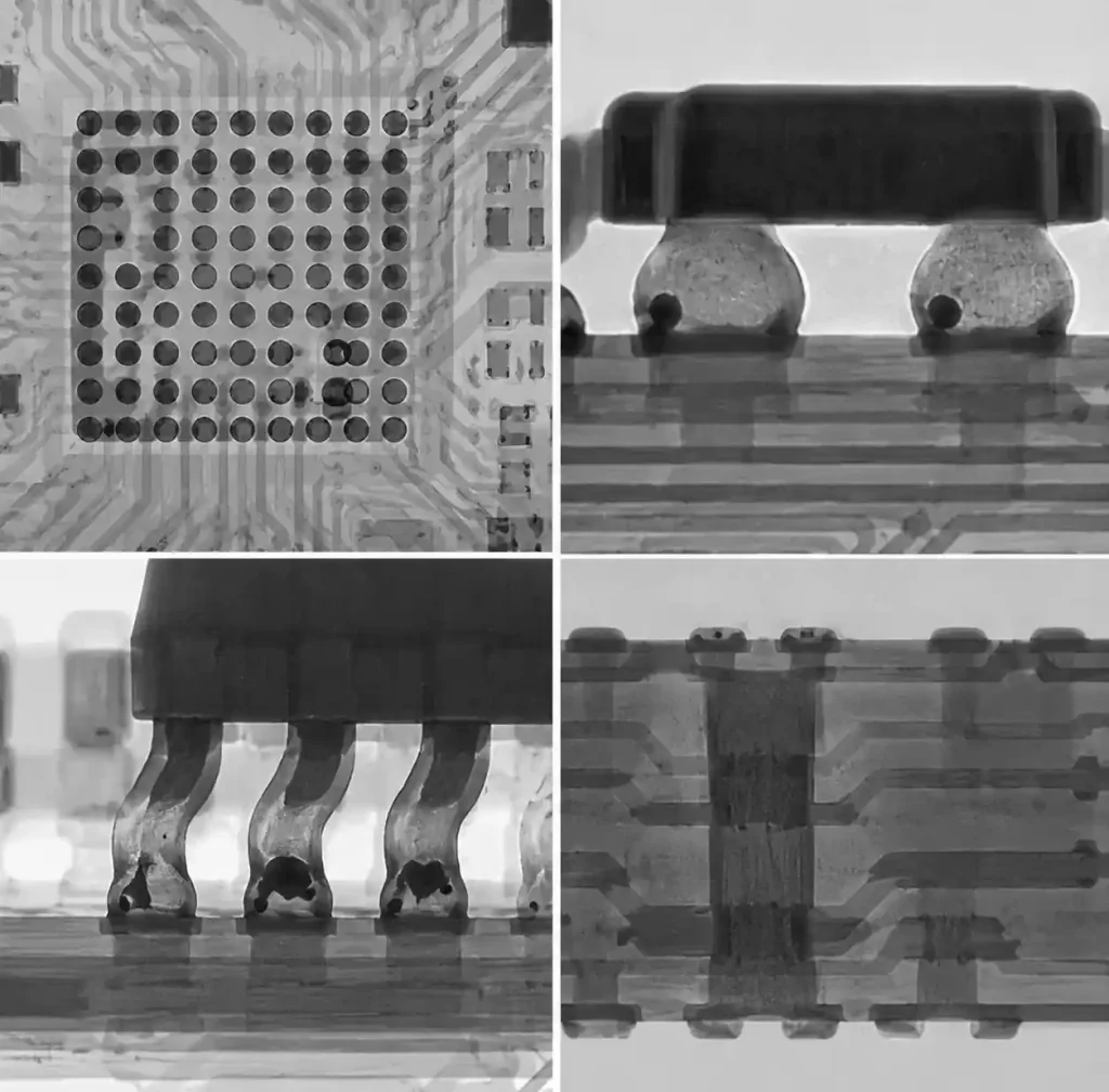
Insufficient solder volume: BGA balls should appear round and uniform. Collapsed or flattened balls indicate insufficient solder, creating high-resistance joints prone to cracking. This occurs when paste volume is too low or reflow profiles don’t achieve proper wetting.
Head-in-pillow defects: The solder ball and paste fail to coalesce during reflow, leaving a void at their interface. This defect became common with lead-free solder and warped substrates—thermal expansion lifts components during reflow.
Buried via voiding: HDI boards with filled microvias can trap voids during plating. A 0.15mm via with 40% voiding creates high resistance that degrades signal rise times or causes intermittent failures under vibration.
Inner layer misalignment: Misregistration can create partial contact between via barrels and inner layer pads, increasing resistance. X-ray reveals via offset relative to pad edges.
QFN solder bridging: Fine-pitch QFN packages with 0.4mm lead pitch can develop bridges completely hidden from optical inspection. X-ray immediately shows abnormal bright connections between adjacent pins.
When X-ray Inspection Is Mandatory vs Optional
Not every assembly requires X-ray. Cost-sensitive consumer products with low-power BGAs and large pitch (>0.8mm) may skip X-ray, relying on AOI and functional test.
X-ray becomes mandatory when:
- BGA pitch <0.65mm—void inspection is the only way to verify quality
- Thermal performance is critical—power devices, RF amplifiers, LED arrays
- Reliability exceeds consumer grade—automotive, medical, aerospace, industrial
- Process qualification—baseline data validates reflow profiles and paste performance
- Rework decisions—verify defects exist before spending hours removing BGAs
For production, 100% X-ray adds 15-45 seconds per board, costing $0.80-2.50 per board. Sampling inspection (10-20%) reduces cost to $0.15-0.50 while catching systematic problems. Learn about comprehensive PCB testing methods.
Automated X-ray Inspection: Production Integration
Manual X-ray requires operators to position boards, adjust magnification, interpret images, and document findings. Throughput ranges from 3-8 boards per hour—adequate for prototypes but unable to scale.
Automated X-ray Inspection (AXI) systems follow preprogrammed recipes. The system loads boards, positions them via fiducial recognition, captures images at specified locations, analyzes using trained algorithms, and outputs pass/fail with defect classification. Modern AXI achieves 180-300 boards per hour.
Learning-based algorithms trained on thousands of images classify defects automatically: voids, insufficient solder, misalignment, bridging, missing components. Accuracy exceeds 95% for common defects.
MES integration enables closed-loop process control. When void percentages trend upward, systems flag engineers before reject rates increase. Statistical process control tracks void percentage, solder volume, and alignment across lots, revealing process drift before failures occur.
For PCB assembly services, AXI demonstrates quality commitment and provides objective evidence for customer reporting.
X-ray Inspection Implementation Best Practices
Implementing X-ray inspection requires more than buying equipment. Process integration, operator training, and documentation determine whether X-ray adds value or becomes a bottleneck.
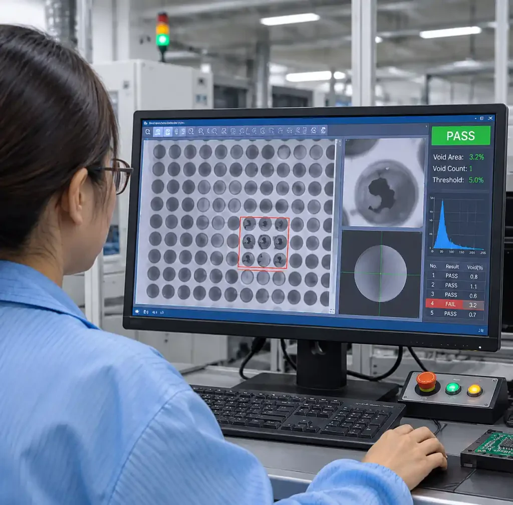
Recipe development: Each assembly requires an inspection recipe specifying locations, magnification, image parameters, and acceptance criteria. Initial creation takes 2-4 hours as you identify critical components and validate against known good/defective samples.
Acceptance criteria: Generic IPC standards provide baselines, but product-specific criteria based on thermal modeling and reliability testing often tighten limits. Document clearly with example images showing acceptable vs rejectable conditions.
Operator training: Effective inspection requires 40-80 hours covering X-ray physics, image interpretation, common defects, measurement techniques, and safety. Automated systems still need trained operators for recipe setup and marginal review.
System integration: X-ray data should flow automatically into quality databases, linking results to serial numbers, lots, and process parameters. This enables traceability and statistical analysis. Review IPC-A-610 classification for documentation standards.
Radiation safety: X-ray systems require proper shielding, monitoring, and operator training. Modern systems with cabinet shielding keep external radiation below background levels, but regulatory compliance requires documentation.
FAQ
Q: Can X-ray inspection damage components or PCBs?
A: No. Industrial X-ray uses 20-160kV energy with 0.5-5 second exposures, delivering doses approximately 1000× below levels affecting electronics. Semiconductor manufacturers use higher energy X-ray during failure analysis without damage.
Q: What void percentage should I target for BGA thermal pads?
A: IPC-A-610 Class 3 allows 25%, but for thermal-critical applications (>2W dissipation), target 10-15% maximum in the central thermal path. Thermal modeling should determine product-specific limits based on junction temperature requirements.
Q: How do I differentiate voids from non-metallic inclusions?
A: True voids appear dark (radiolucent) within bright solder with smooth boundaries. Non-metallic inclusions show intermediate grayscale. Artifacts from scattered radiation create patterns that don’t correlate with physical features. Multiple viewing angles resolve ambiguous cases.
Q: Can 2D X-ray measure voids in double-sided assemblies?
A: 2D measures total void area but cannot separate top-side from bottom-side when components overlap. For double-sided BGAs, laminography or CT provides accurate per-side measurement. If components don’t overlap, 2D remains sufficient.
Q: How often should X-ray equipment be calibrated?
A: Perform functional verification daily using a standard reference artifact. Full calibration including geometric magnification, grayscale linearity, and resolution verification should occur quarterly or after maintenance. Document all calibration per ISO 9001.
Q: What is the smallest void X-ray can detect?
A: Detection depends on system resolution, contrast, and noise. Modern microfocus systems resolve voids down to 10-20 microns under optimal conditions. Practical detection for production ranges from 25-50 microns depending on image quality.
Conclusion
X-ray inspection transforms hidden risks into visible, measurable, actionable data. BGA voiding, buried via integrity, inner layer registration, and thermal pad quality—these failure mechanisms remain invisible to optical inspection yet determine whether products survive qualification testing or fail in the field.
The technology has matured beyond expensive failure analysis tools into production-ready automated systems that integrate seamlessly with high-volume manufacturing. At Andwin Circuits, our automated X-ray inspection systems screen every BGA joint in automotive and medical assemblies, preventing defects that would cost 50-200× more to catch during functional test or field failure.
Don’t wait for field failures to prove the value of X-ray inspection. For BGA assemblies below 0.65mm pitch, thermal-critical designs, and high-reliability applications, X-ray isn’t optional—it’s the difference between shipping quality and shipping hope.