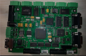
At present, electronic equipment is still used in printed circuit boards as the main assembly method for various electronic devices
and systems. The practice has proved that even if the circuit schematic design is correct,
improper design of the printed circuit board will also have an adverse effect on the reliability of electronic equipment.
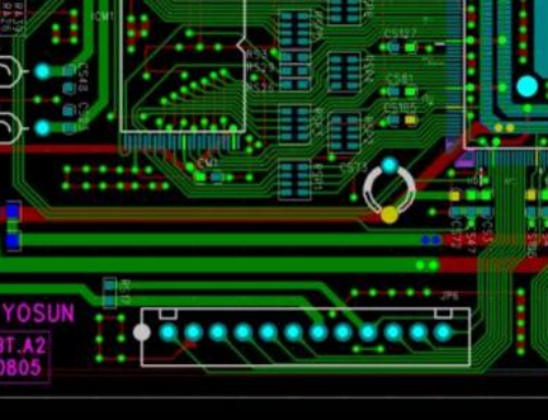
For example, if the two fine parallel lines of the printed board are in close proximity, a delay in the signal waveform is formed,
and reflection noise is formed at the end of the transmission line.
Therefore, when designing a printed circuit board, it is recommended that grounding be an important method of controlling interference.
If you can use the correct combination of grounding and shielding, you can solve most of the interference problems.
The ground structure of the electronic device is roughly systematic, chassis ground (shielded ground),
digital ground (logical ground), and analog ground. The following points should be noted in the grounding design:
1. The correct choice of single-point grounding and multi-point grounding In low-frequency circuits,
the operating frequency of the signal is less than 1MHz, its influence on the inductance between the wiring and the device is small,
and the circulation current formed by the grounding circuit has a greater impact on the interference,
and should be used Grounded at one point. When the operating frequency of the signal is greater than 10 MHz,
the impedance of the ground wire becomes very large. At this time, the resistance of the ground wire should be reduced as much as possible, and the multi-point grounding should be used nearby. When the operating frequency is from 1 to 10 MHz,
if a point is grounded, the length of the ground wire should not exceed 1/20 of the wavelength.
Otherwise, the multi-point grounding method should be adopted.
2. Separate the digital circuit from the analog circuit. There are both high-speed logic circuits and linear circuits on the circuit board. They should be separated as much as possible, and the ground lines of the two should not be mixed.
They are connected to the power supply ground. Try to increase the grounding area of the linear circuit.
3. Try to make the grounding wire as thick as possible. If the grounding wire is very thin,
the grounding potential changes with the change of the current, causing the timing signal level of the electronic equipment to be unstable and the anti-noise performance to deteriorate.
Therefore, the ground wire should be as thick as possible so that it can pass three allowable currents on the printed circuit board.
If possible, the width of the ground wire should be greater than 3mm.
4.When the ground wire is used as a closed-loop design for a printed circuit board consisting of a digital circuit only,
making the ground wire a closed loop can significantly improve the noise immunity. The reason for this is that there are many integrated circuit components on the printed circuit board, especially when there are many components that consume too much power, due to the limitation of the thickness of the grounding wire, a large potential difference will be generated in the ground junction,
and the anti-noise ability will decrease. If the grounding structure is looped, the potential difference will be reduced and the anti-noise capability of the electronic equipment will be improved.
Alice Lu
Email: sales16@andwinpcb.com


