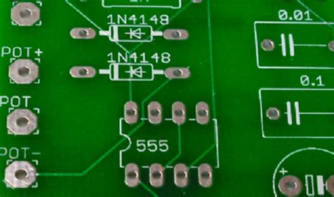
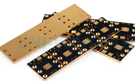
1 layer pcb protoype
What is pcb board prototype
A PCB prototype board is essentially an early sample of a product, with the primary purpose of testing the functionality of the design concept. Designers and engineers use different types of PCB prototypes to test various aspects of a chosen design. Although most prototypes are only meant to test basic user functionality, the PCB prototype board still needs to be functional to some extent since the PCB prototype is meant to test the overall functionality of the design.
Advantages of PCB prototyping boards
1.Shorten time and save costs
During the PCB design process, engineers go through many iterations before creating the final product, which can lead to excessive time. However, PCB prototyping boards can help speed up the entire design and manufacturing process through the following pipeline
1) Complete the test
PCB prototype boards can help PCB design engineers quickly and accurately test design issues. Without this, discovering design flaws will take more time, potentially leading to unhappy customers and lost revenue if not delivered in a timely manner.
2) Customers see the product in advance for better communication
Customers often want to see the product at more points during the production process and are provided with prototypes to assist with better design. It also minimizes communication with customers and the time they need to redesign.
3) Minimize rework
PCB prototype board testing allows boards to be inspected and tested before production, reducing rework. If a defective product goes into production, it will take longer and cost more in the later stages.
2.Ability to detect defects as quickly as possible
Prototyping can identify design flaws early in the product development process and make factory changes early in the process to avoid a host of potential issues that can affect every aspect of the project.
3.Ability to test components individually
For complex PCB-based project components, it is very useful to test different components individually. By verifying each component individually, any issues that may arise can be identified.
4.Reduce costs
PCB prototype versions can reduce the overall cost of the project, identify issues faster, and resolve issues before mass production runs.
5.Improve the final product
PCB prototyping helps improve each PCB and component, resulting in higher quality designs.
Prototype board type
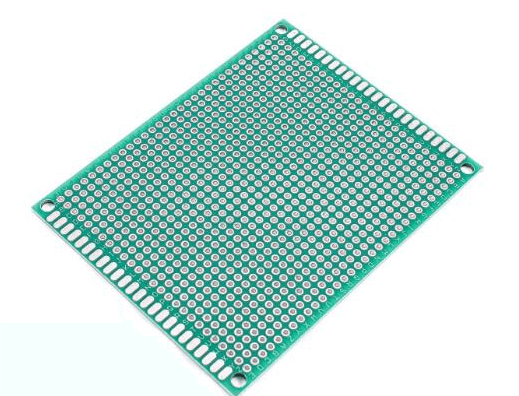
1.Solderless Breadboard
The solderless breadboard allows all electronic components to be assembled according to the design concept and connected through jumpers. There are no soldered connections in this prototype board. This makes replacing, adding or removing any electronic component quick and easy. Additionally, rapid testing is possible because the time required to assemble components is reduced.
Breadboard has a matrix of small holes for assembling components. The holes have a metal coating that allows electrical conduction. These breadboards are made of plastic, and some may also be made of wood.
2.Solder the prototype board
Welded breadboards, also known as soldered prototyping boards, are similar in appearance and appearance to solderless breadboards. However, this can withstand welding. This means one can assemble electronic components and solder them to create a tight connection. These are usually made from wood or silicon instead of plastic.
3.Covered wire board
Winding plates require welded components. All components on the upper surface are soldered and connected using wires on the lower surface. These are similar to soldered breadboards, but offer better reliability. This way, novice hobbyists can use a wire-wrapped board to safely test their design ideas. However, wire packaging boards are less popular and have limited availability in most retail markets.
4.Etch circuit board
These are the most difficult to use. The use of etched circuit boards requires the PCB to be printed and etched onto a hard surface (circuit board) made of wood, silicon, etc. In addition, these boards need to be etched with special chemicals to form an insulating coating on top to protect the board. For this reason, etched circuit boards are only suitable for advanced users.
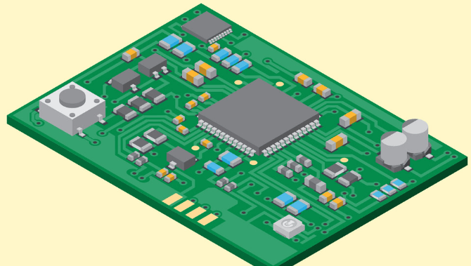
On a PCB prototype board, one can assemble all the electronic components, connect them, and test the initial prototype for errors and functionality. Once a prototype or sample passes all validity and validation tests, the product is marked as suitable for mass production and safe for use. PCB prototype boards are used to test whether product design concepts are suitable for use.
The basic steps and precautions of single-layer PCB prototyping are important knowledge that electronic engineers must master when developing and testing new circuits.
First, the first step in designing a single-layer PCB prototype is to clarify the functional requirements and design goals of the circuit. This includes determining the circuit’s inputs, outputs, and the specific functions of each component. Through detailed requirements analysis, engineers can ensure that the designed circuit will meet the expected performance requirements.
Next, choosing the right materials and components is crucial. Single-layer PCBs usually use FR4 material, which has good insulation properties and mechanical strength. Additionally, component selection should be based on the circuit’s operating frequency, power requirements, and environmental conditions.
Choosing the right components can not only improve the reliability of the circuit, but also simplify the subsequent design and manufacturing process.
After completing the selection of materials and components, engineers need to draw the circuit schematic diagram. The schematic diagram is the basis of PCB design.
It describes in detail the electrical connection relationships between various components. When drawing a schematic, engineers should pay attention to the layout and connection of components to ensure that the circuit functions and performs as expected.
Then, enter the PCB layout design stage. Layout design is to convert the schematic diagram into the actual PCB board diagram. This step needs to consider factors such as signal integrity, power distribution, and heat dissipation.
Engineers should shorten the signal path as much as possible to avoid signal interference, and reasonably arrange the distribution of power and ground wires. In addition, the placement of components should also take into account the convenience of subsequent welding and testing.
After completing the PCB layout design, it is essential to conduct a design rule check (DRC). DRC can help engineers identify potential problems in the design, such as short circuits, opens, and improperly sized vias.
Through DRC, engineers can promptly correct errors in the design to ensure that PCB manufacturing and assembly proceed smoothly.
Finally, the PCB prototype is manufactured and tested. During the manufacturing process, engineers should choose a reliable manufacturer and provide detailed manufacturing documents such as Gerber files and drilling files.
After PCB manufacturing is completed, functional testing and performance verification are critical steps to ensure that the circuit is working properly. Through testing, engineers can discover and correct problems in the circuit and further optimize the design.
To summarize, single-layer PCB prototyping involves several key steps and considerations. Engineers can effectively develop high-quality single-layer PCB prototypes by clarifying requirements, selecting appropriate materials and components, drawing schematics, performing layout design, performing design rule checks, and manufacturing and testing.
These steps not only ensure the functionality and performance of the circuit, but also lay a solid foundation for subsequent mass production.